1 Introduction
Viewing through a color liquid crystal display (LCD) is one of the important features of a digital camera over a conventional camera. It solves the inconvenience of using a viewfinder to view the scene, and can be viewed at the shooting scene by using the liquid crystal display to play back the newly taken photo. The effect of shooting [1] determines whether or not to leave this photo, which gives the photographer better control over the quality of the photo. Therefore, framing and playback with a liquid crystal display are two essential functions of a digital camera. At the same time, the liquid crystal display is also used to display menus and provide a good human-computer interaction interface. The liquid crystal displays used in digital cameras currently on the market are color TFT liquid crystal displays, which solve the phenomenon of adjacent pixel crosstalk in general liquid crystal displays [2], so they can be used to display real moving images.
The main function of the liquid crystal display control circuit in the digital camera ASIC chip is to provide all necessary control timing signals to the liquid crystal display module (LCM) and the digital-to-analog converter, and accept image data from the YCbCr format of the system, and then perform The color space transform converts the image into an RGB format, and then outputs the image data to the off-chip DAC in a color of each pixel in a certain order.
2 system structure and design requirements
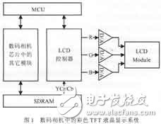
Figure 1 shows a schematic diagram of the LCD display portion of the digital camera system chip we designed. According to the system requirements of the design of the integrated circuit chip of the digital camera, the liquid crystal display control circuit can be used to control a variety of liquid crystal display modules, from more than 60,000 pixels to more than 200,000 pixels. This circuit has two modes of operation: framing mode and playback mode, which display dynamic and still images, respectively. At the same time, the circuit has a variety of scanning methods - there are four combinations of up and down and left and right. Therefore, this circuit must have a high degree of flexibility, which can be programmed by the system to control its operating state.
3 circuit design
According to the design requirements, we first determine the overall framework of the circuit, then design each module and describe it in Verilog HDL language, and finally perform RTL level simulation. Figure 2 is a functional block diagram of the entire circuit.
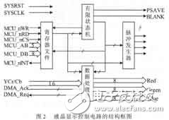
The entire liquid crystal display control circuit consists of four modules, a register file, a finite state machine, a data processor, and a pulse generator. The signal line of this circuit is mainly related to three circuits, one is related to MCU interface circuit, including MCU_AB (address bus), MCU_DB (data bus), MCU_nWR (write enable), MCU_nRD (read enable) and MCU_nCS (MCU) The operation selects the signal); the second is related to the liquid crystal display module and the digital-to-analog converter, including the timing signal output from the pulse generator for controlling the entire image display and the three primary color data of red, green and blue, and the three control DACs of PSAVE, BLANK and D_CLK. The converted signal; the third is connected to other sub-modules in the digital camera ASIC chip, including DMA_Req1, DMA_Req2, DMA_Ack1, DMA_Ack2 four DMA operation interaction signals and 16-bit YCbCr data signals. SYSRST and SYSCLK are system reset and clock signals, respectively. The design of each module is analyzed separately below.
3.1 Register File Module
The register file module is mainly composed of two parts: an MCU interface and a register array. The MCU interface system can read and write the register array, so that the liquid crystal display control circuit has the characteristics of flexibility and variety, can control a variety of liquid crystal display modules, and works in multiple modes, and can output various scanning modes. The control signal can display the image in any area of ​​the display, and also has a software reset function. The entire register array consists of 30 8-bit registers divided into three main categories: mode register, status register, and waveform parameter register. The lower 7 bits of the mode register are valid, as shown in Figure 3.

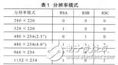
The 0th bit is the status/reset bit, which is output to the MCU and connected to the reset terminal of the flip-flops of other modules in the LCD display control circuit. This bit is 1 at system reset and display end, indicating idle and putting the interface in reset. If the system sets this bit to 0, the reset state of the circuit is released and is active. The first and second digits are used to determine the scanning mode when displaying, where V_DIR indicates the frame scanning mode. This position 1 indicates scanning from top to bottom, and 0 indicates scanning from bottom to top; H_DIR indicates the scanning mode, setting and setting 0 indicates scanning from left to right and right to left, respectively. There are four scanning modes for the two combinations. The three bits RSA, RSB and RSC are used to indicate which type of liquid crystal display module is used, and their combinations and corresponding display resolutions are shown in Table 1. The MODE bit is used to indicate the operating mode, 1 means working in the framing mode, and 0 means working in the playback mode.
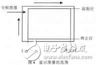
The status register includes a row number register, a column number register, a start row register, a termination row register, a start column register, a termination column register, and a color sequence register of the parity row. The row number and column number registers set the number of vertical clock pulses required to display one frame of image and the number of horizontal clock pulses required to scan a line of images. The two register parameters are different for different specifications and brands of liquid crystal displays. The start row register, the termination row register, the start column register, and the termination column register set the range of the display image, as shown in Figure 4, which enables design requirements for displaying the image in any area of ​​the display. Since the TFT color liquid crystal display displays only one of the three primary colors for each pixel, it displays the color effect together with the adjacent pixels, so the order of the colors of the odd and even lines is different. In order to ensure that the correct primary color data signal is given at a certain pixel point, in a certain scanning mode, the start row register and the start column register must coincide with the color sequence register of the parity row. For example, with the 280 & TImes; 220 model LCD display, the odd color order of the odd lines is RGB and the even line color order is GBR when V_DIR=0 (scan from top to bottom) and H_DIR=1 (scan from left to right). This color sequence must be guaranteed when setting the start line register and the start column register for proper display.
The pulse parameter register sets the time parameter of each drive pulse waveform, and several registers correspond to one phase drive pulse. When the state of the row counter and column counter in the finite state machine module is the same as the setting of some pulse parameter registers, the corresponding output pulse is inverted. These parameters are different for different specifications and brands of liquid crystal displays, even for the same product, they are different in different scanning modes.
3.2 finite state machine module
The finite state machine consists of two 16-bit row and column counters, and the state variable is the state/reset bit of the mode register. In the operating mode, the two counters cycle through. When the row counter state is the same as the start row register, the row valid signal goes high, indicating that the display of the frame image begins, at which point the data processor module begins to operate. The row counter is reset when the system reset or row counter state is the same as the termination row register. After the row valid signal goes high, when the column counter state is the same as the start column register, the pixel valid signal goes high, indicating that the effective display of the row begins, at which point the data processor begins to output the color data for each pixel. The column counter is reset when the system reset or column counter status is the same as the termination column register.
3.3 Data Processor Module
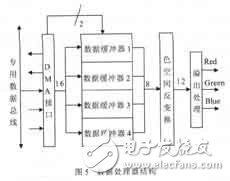
The data processor module is shown in Figure 5. It consists of three parts: the DMA interface and its data buffer, color space inverse transform circuit and overflow processing circuit. According to the system design requirements, the original image sampled by the charge-coupled device (CCD) image sensor is transformed into a YCbCr format image after interpolation and color space conversion by the pixel processor module. According to the JPEG standard, the color from RGB to YCbCr The spatial transformation follows the formula [3](1).
Y=0299R+0587G+0.114B
Cb=_0.169R-0.331G+0.5B (1)
Cr=0.5R-0.4186F-0.0814B
At the same time, for the convenience of storage, the transformed Y signal is subtracted by 128, so that the values ​​of the three signals are between -128 and +127, and thus can be represented by 8-bit signed numbers. When the YCbCr signal is stored, the pixel processor module averages the chrominance signals of adjacent pixels and then multiplexes them, thus saving storage space. Therefore, the luminance signals of two adjacent pixels in the image memory are combined into a 16-bit data and stored in a storage unit, and the multiplexed chrominance signal is used.
The number is stored in the unit of the next address [3]. When the liquid crystal display is to be used for image display, the luminance signal and the chrominance signal of two pixels are obtained by two consecutive DMA read operations, respectively placed in the 16-bit data buffers 1 and 2, and then read new. The YCbCr signals of two adjacent pixels start to process the data in buffers 1 and 2 while placing them in data buffers 3 and 4, thus implementing a simple pipeline operation by the action of two pairs of data buffers. In the inverse transformation of color space, the RGB signal required to convert the YCbCr signal into liquid crystal display is realized. According to formula (1) and simplified, we can obtain the corresponding inverse transformation formula (2).
 (2)
(2)
Based on the range of the inverse transform coefficients, we multiply all the coefficient values ​​by 64 and then represent the integer part of the product with an 8-bit signed number. In the inverse of color space, we design a Booth multiplier of 9&TImes; 8 to implement signed multiplication of chroma signals and transform coefficients. In order to ensure the correctness of the inverse transform, the symbol expansion is performed during the operation, so the RGB signal obtained by the transform is a 12-bit signed number, and the data finally output to the digital-to-analog converter is an 8-bit unsigned number, so Perform overflow processing and limit all calculation results to the range of 0~255. At the same time, since the potential of the common electrode of the liquid crystal display is an alternating potential, that is, the potentials of the common electrodes of two adjacent rows are inverted, the image data of two adjacent lines should be outputted with the original code and the inverted code, respectively.
3.4 Pulse Generator Module
The pulse generator generates respective driving waveforms according to the state of the row and column counters in the finite state machine and the parameters in the waveform parameter register, and these driving waveforms are used to drive the liquid crystal display module itself and its external analog front end circuit.
4 Verilog language implementation and FPGA hardware verification
After determining the overall design of the functional modules, you can use the Verilog HDL language to model the RTL design, and then use Synopsys' VCS to simulate and debug the design. After the RTL-level simulation, we performed hardware verification of the FPGA for this circuit. The chip used was Xilinx's Virtex E1000-BG560, and the system clock was 54MHz. Whether it is a separate test or as part of a dedicated chip for the entire digital camera, the liquid crystal display control circuit can successfully achieve the design requirements in two working modes with good performance.
5 Conclusion
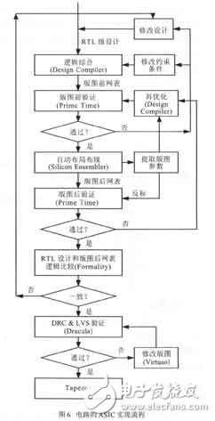
After verification by FPGA, the liquid crystal display control circuit is realized by TSMC 0.25mm SAGETM process. The back-end process is shown in Figure 6. Among them, Design Compiler, Prime TIme and Formality are products of Synopsys; Silicon Ensembler and Virtuso are products of Cadence. . The circuit sampling interface has a circuit scale of about 15,000 gates and a chip area of ​​0.49 mm & TImes; 0.8 mm.
Half Cell Module,Solar Q Cells,Solar Pv Module,Monocrystalline Half Cell Module
Jiangxi Huayang New Energy Co.,Ltd , https://www.huayangenergy.com
