Abstract: Introduce the hardware and software design of the analog telephone voice card in the multimedia gateway. An analog telephone voice card design based on the TMS320VC5402 processor, AM79 (SLIC) user line interface chip and AM79Q02 (SLAC) user audio processing chip and PCI9052 PCI bridge chip.
At present, hotspot CTI (computer telephony integration) applications include media gateways, IP phones, and IP fax. Softswitch is sometimes called a call server or media gateway controller. The basic concept of softswitch is to separate the call control function from the transport layer (media gateway). The basic call control functions such as call routing, management control, and signaling interworking are realized through the software on the server. Because call control is separated from call transmission, separate planes are established for control, switching, and software programmable functions, so that service providers can easily combine transmission services with control protocols to achieve service transfer.
The telephone voice card is the basis for constructing various CTI application systems. It is a computer plug-in used for computers and capable of voice processing. The main functions of the telephone voice card (referred to as the voice card) are: connecting to the telecommunications network through a computer, providing dialing, ringing detection and control off-hook, signaling detection, transfer internal line, monitoring recording, fax, data transmission, calling number Detection and other service functions. As a functional component for voice processing, voice cards generally have an interface with the telephone network. Different interface types from the telephone network can be divided into analog voice cards and digital voice cards. 
The following will introduce an analog telephone voice card design based on the TMS320VC5402 processor (DSP5402 for short), AM79R79 (SLIC) user line interface chip and AM79Q02 (SLAC) user audio processing chip and PCI9052 PCI bridge chip.
1 Overall system plan
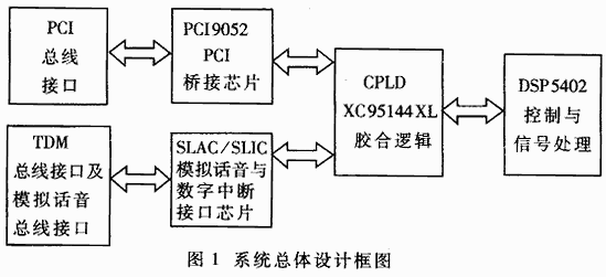
In the design, the telephone voice card realizes the continuous control and framing of 16 channels of voice. The system interacts with the DSP5402 through the PCI bus to maintain and manage the board; the voice service is connected through the TDM (Time Division Multiplexing) bus; the DSP5402 completes the connection control and framing of the voice inside the board. The overall design block diagram is shown in Figure 1.
2 Design of hardware circuit
2.1 Introduction to DSP5402
DSP5402 is TI's 54x series 16bit fixed-point DSP, which has the characteristics of low power consumption and high cost performance. The specific features are as follows: the extended address mode can be addressed up to 1M × 16bit external program space, 4K × 16bit on-chip ROM, 16K × 16bit on-chip dual-port RAM; the instruction set supports single instruction loop and block loop, and storage block movement instructions provide efficient programs And data memory management; on-chip hardware resources include software programmable wait state generators and programmable memory cell conversion, phase-locked loop (PLL) clock generators connected to internal oscillators or external clock sources, and two multi-channel buffered serial ports (McBPs ), Enhanced 8bit parallel host interface (HPI8), two 16bit timers, 6-channel direct memory access (DMA) controller; working power supply has 3.3V and 1.8V (core); power supply at 3.3V (1.8V core voltage ) The execution cycle of the fixed-point instruction for placing a single cycle can reach 10ns (100MIPS).
In the design, DSP5402 completes the communication and data exchange with the host through the PCI bus on the one hand, on the other hand, completes the control of the connection and framing function of the voice, and the signal and signaling processing function. 
Therefore, the peripheral design of DSP5402 is divided into two parts:
(1) The hardware interface between DSP5402 and PCI9052
The completion of the DSP5402 HPI bus and PCI9052 LOCAL local bus connection, the host can thus communicate with the DSP5402 through the PCI bus. First load and start the DSP5402 through HPI, and then complete the monitoring operation of the voice board.
When DSP5402 exchanges information with the host (HOST), HPI is a peripheral device of the host. It has the following characteristics: can access all on-chip RAM space, HOST access is always synchronized with the DSP5402 clock, HOST and DSP5402 can access on-chip RAM.
The PCI bus control chip PCI9052 of PLX Company completes the information interaction between the PCI bus high-speed signal and the local device resources on the LOCAL side. It provides the interface between the local bus and the PCI bus, avoids users from directly facing the complex PCI bus protocol, and provides high-performance connection from the target PCI interface board to the PCI bus; supports a wide range of local buses, up to 132 Mbps transmission rate; programming PCI9052 can realize multiplexed / non-multiplexed 8-bit, 16-bit, 32-bit local bus interface.
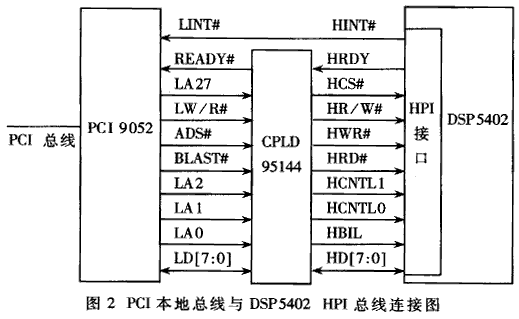
In the design, the PCI9052 local bus uses a non-multiplexed 8-bit mode to match the HPI8 bus. CPLD completes the interconnection of the PCI local bus and the HP540 bus of the DSP5402, as shown in Figure 2. The specific signals are defined as follows: PCI local side address signals (LA27, LA0, LA [1: 2]), cooperate with PCI local side read / write signal LW / R #, address enable signal ADS # and BLAST transmission mode enable signal Encoders have intentional HPI control signals (such as chip selection signal HCS #, data word high and low byte selection signal HBIL, function register selection signal HCNTL [0: 1], and read and write signals HRD #, HWR #); HPI ready signal HRDY is generated The PCI local ready signal READY # can be inserted into the waiting cycle as required to meet the actual timing requirements; the HPI interrupt signal HINT # triggers the PCI local interrupt signal LINT #; the HPI data bus HD [0: 7] matches the PCI local through CPLD level matching The side data bus LD [0: 7] is connected. 
(2) The hardware interface between DSP5402 and AM79Q02 (SLAC)
The AMD company's SLIC subscriber line interface chip AM79R79 (SLIC for short) is selected to realize the transition of the telephone connection status, monitor the load change of the telephone line, realize off-hook detection, feed supply and ringing transmission; SLAC users who realize seamless interface with it The audio processing chip AM79Q02 (abbreviated as SLIC) realizes the continuous state transition of the telephone, monitors the load changes of the telephone line, realizes off-hook detection, feed supply and ringing transmission; the SLAC user audio processing chip AM79Q02 (which implements seamless interface with it (SLAC for short) realizes A / D conversion of voice and framing into PCM code stream. SLAC) A / D conversion of voice and framing into the PCM stream. The SPI MCU bus interface provided by SLAC simplifies the hard-wire connection with the MCU, and SLAC (providing a complete SLIC control bus) and SLIC can be seamlessly connected, so the control of SLIC can be completely simplified to directly control SLAC to complete indirectly , Simplify the design of the hardware circuit, saving the user's development costs.
The SPI interface includes clock DCLK, chip select CS and data line DI / O, but there is no read and write direction control line. The control of the read and write direction is completed by writing bit0 of a single byte read and write command word; bit7-bit1 contains the address information of the control register, so that the register operation of SLAC can be completed.
In addition, special attention should be paid to the timing of designing the SPI interface of SLAC: each read and write operation CS low enable is effective to maintain at least 8 DCLK cycles, that is, a byte read and write operation is completed; when CS low enable is effective, 8 DCLK hands During the period, the reading and writing are ignored; when CS low enables effectively 8 to 15 DCLK cycles, the last 8 DCLK cycles are taken as effective read and write cycles; when CS low enables effectively more than 15 DCLK cycles, then Will cause a hardware reset.
Figure 3 is a timing diagram of SLAC's MCU interface SPI bus.
DSP5402 has two channel buffer serial ports (McBPs). McBPs have multiple configuration modes, which can be configured as high-speed master-slave SPI interface products as needed. Taking into account the future functional expansion needs, McBPs are retained in the design; adopting software to read and write general I / O, simulating SPI timing and implementing SPI interface with CPLD, thus completing the hardware interface between DSP5402 and SLAC, and implementing DSP5402 status monitoring and control of SLAC / SLIC unit.
2.2 PCI9052
PCI9052 is a PCI bus slave interface chip introduced by PLX. It provides a convenient interface between the local bus and the PCI bus. Avoid users directly facing the complex PCI bus protocol.
2.3 AM79Q02 and AM90R79
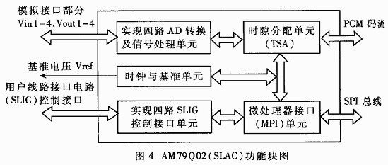
Select AMD SLIC / SLAC subscriber line interface and audio processing, framing circuit. SLIC realizes the conversion of the connection status of the telephone, monitors the load changes of the telephone line, and realizes the functions of off-hook detection, power supply and ringing transmission; and SLAC realizes the A / D conversion of the voice and framing to 8Mbps PCM code In the stream. It also has the following characteristics: soft configuration SLIC input impedance, transceiver gain, loop loss and other line parameters; A / μ rate coding or linear coding is optional; PCM code stream time slot redistribution; single and dual 8Mbps PCM channels are optional; support Four-way SLIC control and voice processing reduce the size and cost of the circuit board; internal loopback and audio generation circuit facilitate circuit fault diagnosis and testing.
SLAC subscriber line audio processing circuit, as shown in Figure 4.
In addition, SLAC communicates with the MCU to provide an SPI interface, which simplifies the hardware connection with the MCU; and SLAC and SLIC seamlessly connect the SLIC control and audio interface, so directly control the SLAC to indirectly complete the control of the SLIC, simplifying the hardware circuit and software programming . 
3 Software design
The software design is divided into the following two parts: driver design and host programming in the target board (including PCI driver and host application development).
3.1 Driver design in target board
The driver in the target board can be divided according to functional modules: system self-test and test module; SLAC / SLIC control module, including line activation, ringing, standby and new line status, off hook detection and programmable detection threshold; and host Communication module, real-time monitoring of the target board by the host.
3.2 Host programming
Here, the host program design is divided into two parts: PCI driver development and host application development.
The PCI driver uses the driver driver software of the Jungo company, KernelDriver, which is very convenient to use. Use the driver generation wizard in KernelDriver to generate driver code as needed; compile the driver CPP code just generated in the MS-VC ++ compilation environment, debugging is no problem, and PCI driver development is completed.
The host application program is based on the PCI driver, and calls related API functions to operate the PCI device, complete the host program loading of the target board, and perform real-time monitoring operations on its status.
In this scheme design, the CPU selects the TMS320VC5402 with high cost performance, and its CCS development environment cooperates with JTAG debugging, which is convenient for development; choose the user line interface chip AM79R79, user audio processing chip AM79Q02, and PCI PCI bridge chip that can be seamlessly connected PCI9052 greatly reduces the difficulty of software and hardware development, speeds up the development process, and achieves the ultimate goal of reducing development costs.

Follow WeChat

Download Audiophile APP

Follow the audiophile class
related suggestion
