The Global Positioning System (GPS) is a navigation system composed of 24 satellites operating in 6 earth orbits. GPS can help users accurately determine their location no matter where they are.
Mobile phones are ideal products with integrated GPS functions. Integrating the GPS receiver into the mobile phone can realize synchronous GPS (S-GPS) applications. At this time, the GPS receiver is used with wireless communication systems of different frequency bands (such as PCS and cellular networks). Consumers hope that GPS-enabled mobile phones can reliably receive and amplify signals transmitted by satellites, because errors in reception will cause errors in location information. Unfortunately, RF interference signals often damage the quality of GPS signals.
System internal interference
The integration of the GPS receiver with other wireless mobile communication transmitters on the same circuit board makes it very susceptible to interference from internal signals of the system, thereby reducing its sensitivity and linearity. When the transmitter is in transmit mode, part of the transmitted signal will leak into the GPS receiving path. The receiver will therefore face a very high total input power and may cause saturation of the receiver's back-end circuit. This will cause a non-linear signal at the back end of the receiver and an error in the signal during reception. In order to avoid this phenomenon, it is necessary to prevent out-of-band transmitted signals from entering the GPS receiving path. Therefore, the GPS receiving path is required to have a good ability to suppress out-of-band transmitted signals. By suppressing the interference signal, the GPS chipset can be prevented from being overloaded due to strong interference power, and can provide linear amplification for the received signal.
Ensure receiver sensitivity and linearity
Designers usually put a filter on each end of the GPS low noise amplifier ( LNA ). The filter in front of the LNA helps to suppress out-of-band signals while preventing the LNA from entering saturation. This filter must have very low insertion loss. A filter with high insertion loss should be avoided before the LNA, because this will increase the noise figure of the system. According to the Friis formula, the total noise figure of the system mainly depends on the noise figure or loss of the first stage. The filter behind the LNA can be used to further improve the out-of-band rejection performance to prevent overloading of the post-stage circuit.
However, in the noise calculation shown in Figure 2, even if the LNA has a particularly good noise figure (0.8dB), placing a pre-filter with an insertion loss as low as 0.5dB in front of it can reduce the cascaded noise figure. Only when the gain is high enough does the cascaded noise figure depend on the first stage circuit. The negative gain of the first stage filter can reduce the cascade noise figure to 1.35dB. Therefore, the solution has three components, including two filters and an LNA.
Simplified S-GPS design
The above solution can be simplified to a solution with only one filter, that is, the LNA with good linearity is taken as the first stage, and the filter with good out-of-band rejection performance is taken as the second stage. This section will detail the "LNA-filter" module suitable for use as a GPS receiver front end. It integrates a low noise, high linearity enhanced pseudomorphic high electron mobility transistor (E-pHEMT) LNA and a low insertion loss high out-of-band suppression thin film cavity acoustic resonator (FBAR) filter. This combination can form a front end with excellent noise figure and good linearity.
E-pHEMT technology can be used to design a highly linear LNA; FBAR technology is used to design a small filter with high Q value, so that it has a very steep roll-off or excellent out-of-band rejection performance. The LNA module with integrated FBAR filter can provide sufficient suppression of cellular and PCS band signals, and helps to improve the performance of receivers working in parallel or concurrent GPS (S-GPS).
The high linearity "LNA-filter" module can handle high input power without compressing the received signal. Therefore, as long as there is sufficient isolation between the GPS path and the PCS / cellular path, the filter in front of the LNA module can be omitted. Without a front-end filter, the noise figure of the system depends on the LNA and can be as low as 0.8dB. This implementation method greatly improves the sensitivity of the receiver.
Due to the narrow bandwidth of the filter, integrating the LNA with the filter can also make the input impedance of the module appear more concentrated (impedance diffusion on the Smith chart is smaller). Compared with a split LNA without a post filter, this solution makes impedance matching between the antenna and the input LNA module easier. The single-chip solution also ensures more reliable and consistent receiver performance.
Analysis and discussion
Figure 3 shows the test setup used for gain compression measurement of GPS signals due to out-of-band interference. Set the power level of the PCS / cellular band signal according to the values ​​shown in the table in Figure 3 to represent the isolation range between the GPS path and the PCS / cellular path. The input power level of the 1.575GHz GPS signal is fixed at -35dBm, while the output power of the PCS / cellular amplifier is + 24dBm. Supplying different input power levels to the input end of the LNA module (or GPS antenna) can change the isolation level. The input power generated by the interference source at the input end of the module can be calculated by the following formula:
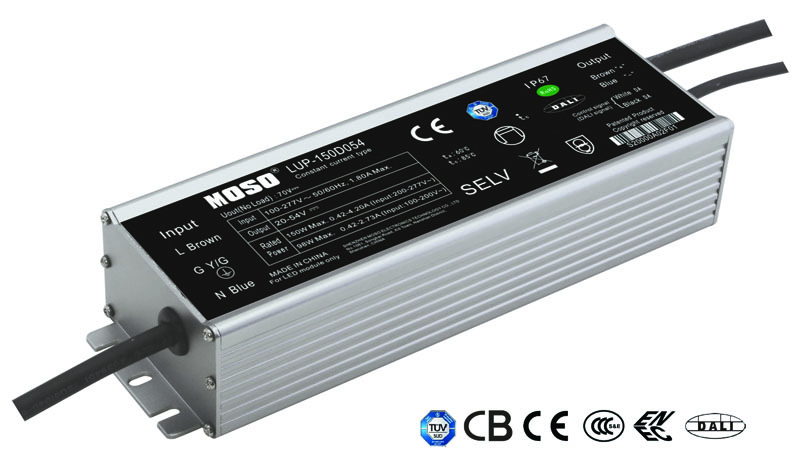
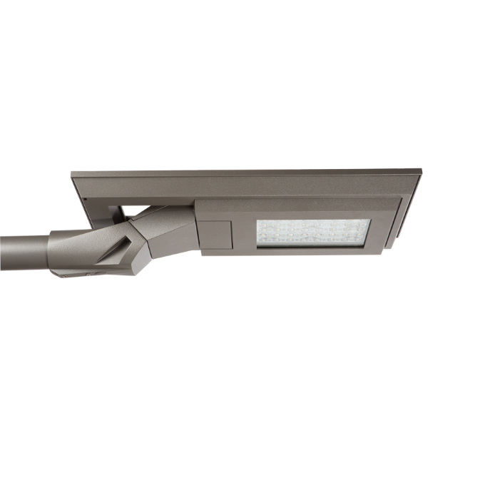
MOSO provide Dim-to-off Led Driver for energy-saving and circuit safety, supporting 0-10V, PWM, timer step dimming or DALI control, with low stand-by power. It is IP67, build-in surge protection, Class II design, power range 75W~320W. Dimming driver can adjust the output by programming software or controller which is isolated with diming signal.


This Dimming driver ensures cool operation and long life with extruded-metal housing and fully glue-potted. It is certified by CCC, CE, TUV, ENEC and CB standards, widely used in street lighting, flood lighting, industrial lighting.
MOSO has set several distributors in Europe, United States, Latin America, Asia and Australia. All MOSO Dim-to-off Led Driver provide 5 years global warranty. In case of any failure, customers can get replacement either from MOSO directly or any one of MOSO distributors.
MOSO always dedicates to providing professional outdoor lighting solutions. Please feel free to contact our sales team if you need any support!
Dim-to-off Led Driver
Dim-to-off Led Driver,Dim-to-off LED Dimmable Driver,Dimmable Dim-to-off LED Driver,Dim-to-Off Timer Dimmable LED Driver
Moso Electronics , https://www.mosoleddriver.com
