The VC5509A includes an I2C peripheral interface for easy communication with the ADXL345. In the commissioning, the laboratory-made DSP motherboard SDUST VC5509A V1.1 was used. The board's JP2 expansion interface leads to the I2C bus. The motherboard also uses the I2C bus to complete the configuration with the AIC23B. However, since the I2C bus can suspend multiple peripherals, there is no need to connect an ADXL345.
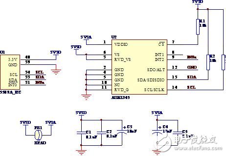
Since the ADXL345 is not easy to solder, the PCB board of Feituo Electronics was purchased when buying the chip. Decoupling capacitors, pull-up resistors, etc. have been added to the PCB. The following figure shows the connection diagram between the VC5509A main board and the ADXL345 module.

Diagram of the connection between ADXL345 and 5509A motherboard (I2C)
Analysis of the schematic diagram, ADXL345 requires 3.3V power supply, directly using the 5509A motherboard to provide, instead of using 5V conversion on the 345 small board, so the 5V pin vacancy can be. The CS pin is left floating because it has been pulled up in the module to indicate communication in I2C mode. Pull SDO down, the I2C address is 0x53 (if the pull-up, the I2C address is 1D). Connect the INT1n output to the INT0n of the motherboard, and connect the SDA and SCL lines accordingly. The U1 pin marked in the figure is the pin number corresponding to the expansion port JP2 on the 5509A main board.
The following picture shows the complete schematic:

ADXL345 and 5509A motherboard connection (I2C) schematic
Summary of debugging points:
1) The interrupt of ADXL345 is active high by default, while the 5509A is active low by default, so start to modify it. Setting the DATA_INVERT bit in the DATA_FORMAT(0x31) register sets it to 1 to indicate active low.
2) Modify the CPLD code to change the INT0 output from 1 to high impedance.
3) It is possible to judge whether the I2C reading is normal by reading the register DEVID. The data in this register is fixed to 0xE5. If the data is read correctly, it indicates that the I2C read function is written correctly.
4) Continuously read the register, there will be a bus busy error, you need to add a necessary delay after reading the data.
5) The debugging summary found that although the 5509A manual states that the external interrupt is active low, it should be valid for the falling edge. Due to the uncertainty of the operating state of the ADXL345, the INT1 output may have been pulled low before the interrupt is enabled. At this time, even if the external interrupt is enabled, the interrupt subroutine cannot be entered as expected. You need to find a way to clear INT1 once, so that you have a chance to trigger an interrupt. Therefore, after the interrupt is enabled, the clear interrupt is implemented by reading the register to trigger the interrupt loop.
6) It is quite time consuming to find the I2C read and write function in CSL. It is observed that it occupies approximately 380,000 instruction cycles, and at a rate of 144 MHz, it consumes approximately 2.6 ms. The data output rate of the set ADXL345 is 200Hz, which is far from being able to follow. In each interrupt, at least 7 read and write instructions are required, and the time spent on this part alone reaches 18.2 ms. That is to say, when using the I2C bus, the data output rate of the ADXL345 can only be set to 50Hz.
7) Finally test, set the rate to 25Hz, observe the interrupt through the oscilloscope, interrupt once every 40ms, corresponding to 25Hz. The low-level time of the interrupt is basically the same, indicating that the interrupt can be entered regularly. Set the rate to 50 Hz, observe the interruption, interrupt once every 20 ms, corresponding to 50 Hz. Entry into the interrupt is also relatively regular. When set to 100 Hz, the interrupt no longer exhibits periodicity, and the low level hold time is also inconsistent. Explain that there is a phenomenon of interrupt nesting. Consistent with the inference.
PoE managed industrial Ethernet Switches are configured with 1-24 10/100BaseTX/802.3af/802.3at compatible Ethernet ports, and each PoE port provides up to 15.4W/30W@48VDC power output. In situations where the utility power supply is inconvenient or the wiring cost needs to be saved [1]
The PoE industrial switch port supports output power of 15.4W and 30W, and conforms to the IEEE802.3af standard. It supplies power to standard PoE terminal equipment through network cable power supply, eliminating the need for additional power wiring. After investigation, the research and development of POE Switches conforming to IEEE802.3aT and IEEE802.3af standards, the port output power can reach 25-30W. In layman's terms, PoE switches are switches that support network cable power supply, which can not only realize the data transmission of ordinary switches. The function can also supply power to the network terminal at the same time.
Industrial Poe Switches,Network Switch Poe,5 Port Industrial Switch,Mini Size 5 Poe Switch
Shenzhen Scodeno Technology Co.,Ltd , https://www.scodenonet.com
