PCB design is a critical step in switching power supply design. It has a great impact on power supply performance, EMC requirements, reliability, and productivity. With the development of electronic technology, the volume of switching power supply is getting smaller and smaller, the working frequency is getting higher and higher, and the density of internal devices is getting higher and higher. This has stricter anti-interference requirements for PCB layout and wiring. A reasonable, scientific PCB design will make your work more effective.
1, layout requirements
The PCB layout is more elaborate, not to just put it on, and squeeze it to finish. The general PCB layout should follow several points:
(1) The first principle of layout is to ensure the wiring rate of the wiring. Pay attention to the connection of the flying line when moving the device, and put the devices with the connection relationship together.
(2) Center around the core components of each functional circuit and arrange it around it. The components should be evenly, neatly and compactly arranged on the PCB circuit board, so that it is not only beautiful, but also easy to load and weld, and easy to mass produce. Minimize and shorten the leads and connections between the components; the oscillating circuit, the filter decoupling capacitor should be close to the IC, the ground wire should be short, as shown in Figure 1.
   Â
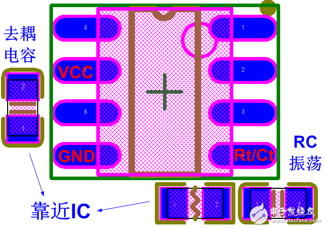
figure 1
(3) When placing the device, consider the subsequent welding and maintenance. Avoid placing short components between the two high-level components, as shown in Figure 2. This is not conducive to production and maintenance. Dense, but with the development of electronic technology, the current switching power supply is becoming more and more compact and compact, so it is necessary to balance the degree between the two, both to facilitate welding and maintenance and to be compact. There is also the need to consider the actual chip processing capability. According to the IPC-A-610E standard, the accuracy of the side offset of the component is considered. Otherwise, it is easy to cause tin between the components, and even the component distance is insufficient due to component offset.
   Â
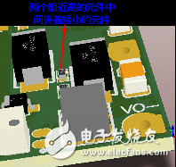
figure 2
(4) Photoelectric coupling devices and current sampling circuits are easily interfered. They should be kept away from strong electric fields and strong magnetic field devices, such as high current traces, transformers, and high-potential pulsation devices.
(5) When the component layout, priority should be given to the loop area of ​​the high-frequency pulse current and the large current, which is reduced as much as possible to suppress the radiation interference of the switching power supply. Several current loops as shown in Figure 3 require special attention.
   Â
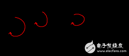
image 3
(6) The area where the high-frequency pulse current flows should be far away from the input and output terminals, so that the noise source is far away from the input and output ports, which is beneficial to improve the EMC performance.
   Â
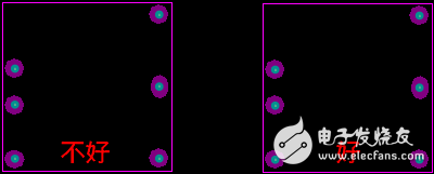
Figure 4
As shown in Figure 4, the transformer on the left is too close to the inlet, and the electromagnetic radiation energy acts directly on the input and output terminals. Therefore, the EMI test does not pass. After changing to the right mode, the transformer is far away from the inlet, and the electromagnetic radiation energy is increased from the input and output end, the effect is improved obviously, and the EMI test passes.
(7) The layout of heating elements (such as transformers, switching tubes, rectifier diodes, etc.) should consider the effect of heat dissipation, so that the heat dissipation of the entire power supply is uniform, and the temperature-sensitive key components (such as IC) should be kept away from the heating components, and the heat is large. The device should have a certain distance from the device that affects the life of the whole machine such as electrolytic capacitors.
(8) Pay attention to the height of the bottom element when laying the board. For example, for a potted DC-DC power module, since the DC-DC module itself is relatively small in size, if the height of the bottom element is unbalanced, the height of the two sides of the pin will be high and low.
   Â
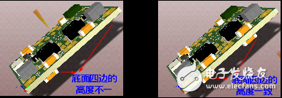
Figure 5
(9) When laying out, pay attention to the antistatic capability of the control pins. The distance between the corresponding circuit components should be sufficient. For example, the Ctrl pin (low level is off), the circuit does not have capacitance like the input and output terminals. Filtering, so antistatic capability is the weakest of the entire module, make sure there is enough safety clearance.
2, the principle of routing
(1) Keep the small signal traces away from the high current traces. Do not approach the parallel traces. If parallelism is not avoided, spread enough distance to avoid interference of small signal traces.
   Â

Figure 6
(2) Key small signal traces, such as current sampling signal lines and signal lines fed back by the optocoupler, to minimize the area enclosed by the loop.
   Â

Figure 7
(3) There should be no long parallel lines between adjacent ones (of course, the same current loop parallel traces are possible), the upper and lower traces should be crossed vertically as much as possible, and the traces should not be suddenly corners (ie: ≤90°) ), right angles and acute angles can affect electrical performance in high frequency circuits.
   Â

Figure 8
(4) The power loop and the control loop should be separated, using a single-point grounding method, as shown in Figure 9 and Figure 10.
The components around the primary PWM control IC are grounded to the IC's ground, then pulled from the ground to the large capacitor ground and then connected to the power ground. The components around the secondary TL431 are grounded to pin 3 of the TL431 and connected to the ground of the output capacitor. In the case of multiple ICs, parallel single point grounding is used.
   Â
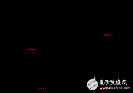
Figure 9
   Â

Figure 10
(5) Do not route the first layer under the high-frequency components (such as transformers and inductors). It is better not to place components on the bottom surface of the high-frequency components. If it is unavoidable, shielded methods can be used. For example, high-frequency components are used. In the top layer, the control circuit is facing the Bottom layer. Note that the first layer of the high-frequency component is shielded by copper, as shown in Figure 11, so that high-frequency noise radiation can be prevented from interfering with the control circuit on the bottom surface.
   Â

Figure 11
(6) Special attention should be paid to the trace of the filter capacitor. As shown in Figure 12, some of the ripple & noise will go out through the trace on the left. The filter on the right will be much better. The ripple & noise will be completely filtered out by the filter capacitor.
   Â

Figure 12
(7) The power cable and the ground wire should be as close as possible to reduce the enclosed area, thereby reducing the electromagnetic interference generated by the cutting of the external magnetic field loop and reducing the external electromagnetic radiation of the loop. The wiring of the power cable and the ground wire should be shortened as much as possible to reduce the loop resistance. The corners should be smooth and the line width should not be abrupt, as shown in Figure 13.
   Â

Figure 13
(8) A large heat-generating component (such as a TO-252 packaged MOS transistor) can be used for heat dissipation in a large area of ​​bare copper, which can improve component reliability. The narrow copper wire of the power trace can be used for tinning with bare copper to ensure the circulation of large current.
3. Safety distance and process requirements
(1) Clearance: The shortest distance along the air measured by two adjacent conductors or one conductor and the surface of an adjacent conductive casing. Creepage distance: The shortest distance measured between two adjacent conductors or one conductor and the surface of an adjacent conductive casing along the insulating surface. If there is limited space in the module PCB and the creepage distance is not enough, you can use the slotting method. As shown in Figure 14, the isolation slot is opened at the optocoupler to meet the good isolation of the primary and secondary. Generally, the minimum slot width is 1mm. If you want to open a smaller slot (such as 0.6mm, 0.8mm), you usually need special instructions to find a PCB manufacturer with high processing precision. Of course, the cost will increase.
   Â
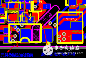
Figure 14
The relationship between the general power module voltage and the minimum creepage distance can be found in the following table:
   Â

(2) The distance from the component to the edge of the board. The components located at the edge of the board are generally not less than 2mm from the edge of the board. For small-sized DC-DC modules such as 10W or less, the size and height of the components are relatively small, and the input and output voltages are not high, in order to meet the miniaturization. At the required time, at least a distance of 0.5 mm or more is required. The distance between the large-area copper foil and the outer frame should be at least 0.20mm or more, which is easy to be milled onto the copper foil during milling and the copper foil is lifted up and the flux is caused to fall off.
(3) If the width of the trace into the round pad or the via is smaller than the diameter of the round pad, teardrops should be added to enhance the adsorption force to prevent the pad or via from falling off.
   Â

Figure 15
(4) When the pins of the SMD device are connected to the large-area copper foil, thermal isolation treatment is required. Otherwise, the heat dissipation is fast during reflow soldering, which may cause soldering or desoldering.
   Â
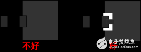
Figure 16
(5) When PCB board is used, it is necessary to consider the feasibility of the board, to ensure that the distance of the component from the edge of the board is sufficient, and also to consider whether the stress of the board will cause the component to be unwound. As shown in Fig. 17, the groove can be appropriately grooved to reduce the stress when the PCB is broken. The position of the component A is parallel to the direction of the V-CUT groove, and the stress is smaller than the component B when the wire is broken; the component C is farther away from the component V than the component A. In the CUT slot, the stress is also smaller than that of the component A when it is broken.
   Â
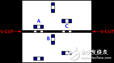
Figure 17
Of course, the above is just a personal summary of some switching power supply PCB design experience, there are many details or other aspects of knowledge need to pay attention to, and finally I want to say that PCB design, in addition to the principle requirements and experience, the most important The point is to be careful and careful, check and check.
Lin Chaowen PCB design PADS entry required course
More than ten years of high-speed PCB design and EDA training experience, PCB designers grow the road classic combat tutorial! 
->> Click to learn about the course right away
Laptop Stand 17 Inch Adjustable,Laptop Stand 17 Inch Alienware,Laptop Stand 17 Inch Bed,Laptop Stand 17 Inch Computer,etc.
Shenzhen Chengrong Technology Co.ltd is a high-quality enterprise specializing in metal stamping and CNC production for 12 years. The company mainly aims at the R&D, production and sales of Notebook Laptop Stands and Mobile Phone Stands. From the mold design and processing to machining and product surface oxidation, spraying treatment etc ,integration can fully meet the various processing needs of customers. Have a complete and scientific quality management system, strength and product quality are recognized and trusted by the industry, to meet changing economic and social needs .
Laptop Stand 17 Inch Adjustable,Laptop Stand 17 Inch Alienware,Laptop Stand 17 Inch Bed,Laptop Stand 17 Inch Computer
Shenzhen ChengRong Technology Co.,Ltd. , https://www.laptopstandsupplier.com
