In accumulates (integrates) at a fixed time interval T1 - constitutes the first "slope", then switches the input of the integrator to a fixed negative reference Vref, causing the integrand to fall back to zero - the second "slope" ", simultaneously measure the time T2 required to do so. The input voltage is:

This design makes some modifications to common algorithms: simply reverse the order of the signal and reference integrals to produce what I call the Reciprocal Double Slope Integral ADC (RDSADC).
Here, Vref is integrated at a fixed time interval T1. The integrator input is then switched to -Vin and the time T2 required to fall back to zero is measured. thereby:

Seeing these two similar equations, you may naturally ask: "What about that?" Look at the following:
In Equation 2, the conversion result is inversely proportional to the time measurement T2 and therefore inversely proportional to 1/Vin, and the differential calculation tells us that the rate of reverse change is changing, but not linear, but the square of the inverse of the measured value, ie:

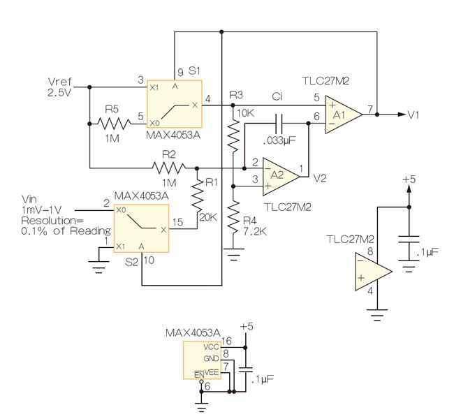
The benefit of this design is that it achieves a non-linear conversion measurement that maintains the high resolution of the low amplitude input without the need for automatic range switching of the Vin scale factor. Figure 1 is an implementation example of an RDSADC. It converts the input in 10-bit resolution, 1mV to 1V range, while maintaining 10-bit resolution in the following two extreme cases: Vin=1V, 1mV resolution; Vin=1mV, 1μV resolution. This means that for T2, a dynamic range of 1000000:1, 20 bits can be achieved with only 15 bit and 32k count resolution. In other words, a 20-bit dynamic range is achieved with a 15-bit count, and the conversion time efficiency is increased by a factor of 32 compared to a conventional DSADC with a similar resolution. In fact, Vin can be from a small point of 0V up to 5V (the resolution is reduced).

Figure 1: The RDSADC reverses the usual integration order to dramatically increase the dynamic range.
How does it work:
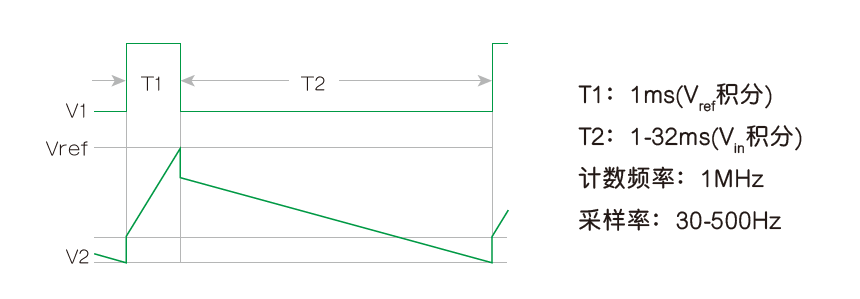
The RDSADC cycle begins at S1 and connects Vref to the "+" input of Integrator A2 (Pin 3) via the R4/(R3 + R4) voltage divider and integrates during time interval T1, ending at V2 = Vref, and Switch the output of comparator A1 to low.

Figure 2: RDSADC timing diagram.
S1 causes the "+" input of A2 to fall close to the reference ground (later later), while S2 switches the "-" input of A2 to near Vin via R1. Then, V2 is decreased with a slope almost proportional to Vin, and the counting interval T2 is determined. When V2 reaches the low threshold of A1, it terminates T2, completes the ADC cycle and starts the next cycle, and continues to cycle.
The savvy reader will notice that during T2, when S1 rejects Vref from the "+" input of A1, R5 produces a positive bias of 42mV. The purpose of this bias is to keep the output of A2 valid until the end of the T2 slash, despite the use of a unipolar power supply.
Also during T2, R2 also produces a valid 32mV bias of 1 to ensure that T2 remains finite (never longer than 32ms), even if Vin is close to zero. thereby:

This idealized calculation ignores real-world biases such as A1 and A2 input offsets, Vref precision, and resistance variations, but these defects can be easily compensated for by simple Vfullscale and Vzero two-point calibrations.
Note 1: 32mV is derived from R1-R2's partial voltage of 2.5V Vref (50mV), which provides 1.6μA (32mV/20kΩ) bias current for Vin/20kΩ input current, minus the voltage divider R3-R5 (18mV) ) Provides a "keep-alive" bias. Therefore, 50mV - 18 mV = 32mV.
Forging is a processing method that uses a forging machine to apply pressure to a metal blank to plastically deform it to obtain a forging with certain mechanical properties, certain shape and size. One of the two major components of forging (forging and stamping)
Forging Parts,Steel Structure Part,Die Hot Forged Part,Cnc Machined Part
Tianhui Machine Co.,Ltd , https://www.thcastings.com
