A successive approximation analog-to-digital converter (ADC) with up to 18-bit resolution and 10 MSPS sampling rate meets the needs of many data acquisition applications, including portable, industrial, medical, and communications applications. This article describes how to initialize a successive approximation ADC for efficient conversion.
Successive approximation architecture
The successive approximation ADC consists of four main sub-circuits: a sample-and-hold amplifier (SHA), an analog comparator, a reference digital-to-analog converter (DAC), and a successive approximation register (SAR). Since the SAR controls the operation of the converter, the successive approximation converter is generally referred to as a SAR ADC.

Figure 1 Basic SAR ADC architecture
After power-up and initialization, a signal on CONVERT initiates the conversion. The switch is closed and the analog input is connected to SHA, which obtains the input voltage. When the switch is turned off, the comparator determines if the analog input (stored at the hold capacitor) is greater or less than the DAC voltage. Initially, the most significant bit (MSB) turns on, setting the DAC output voltage to an intermediate level. After the comparator output is asserted, if the DAC output is greater than the analog input, the successive approximation register will turn off the MSB; if the output is less than the analog input, it will remain on. This process is repeated for the next most significant bit, and the MSB is turned off if the comparator determines that the DAC output is greater than the analog input; it remains on if the output is less than the analog input. This binary search process will continue until each bit in the register is tested. The resulting DAC input is a digital approximation of the sampled input voltage and is output by the ADC at the end of the conversion.
Factors related to SAR conversion code
This article discusses the following factors related to a valid first conversion:
Power Sequence (AD765x-1) Access Control (AD7367) RESET (AD765x-1/AD7606) REFIN/REFOUT (AD765x-1) Analog Input Settling Time (AD7606) Analog Input Range (AD7960) Power Save/Standby Mode (AD760x) Delay (AD7682/AD7689, AD7766/AD7767) Digital Interface Timing Power SequenceADCs with multiple power supplies have a clear power-up sequence. The AN-932 application note power sequence is a good reference for the design of these ADC power supplies. Special attention should be paid to analog and reference inputs, as these should generally not exceed 0.3 V of the analog supply voltage. Therefore, AGND – 0.3 V “VIN†VDD + 0.3 V and AGND – 0.3 V “VREF “VDD + 0.3V. The analog supply should be turned on before the analog input or reference voltage, otherwise the analog core may be powered up in a latched state. Similarly, the digital input should be between DGND − 0.3 V and VIO + 0.3 V. The I/O supply must be turned on before (or at the same time as) the interface circuit. Otherwise, the ESD diodes on these pins may become forward biased and the digital core may be powered up in an unknown state.
Data access during power ramp
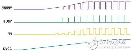
Do not access the ADC until the power supply is stable, as this may put it into an unknown state. In the example shown in Figure 2, the host FPGA is attempting to read data from the AD7367, while the DVCC is ramping up and the result may cause the ADC to enter an unknown state.

Figure 2 Reading data during DVCC ramp up
SAR ADC initialization by reset
Many SAR ADCs (such as the AD760x and AD765x-1) require initialization via RESET after power-up. After all power supplies have stabilized, a specified RESET pulse should be applied to ensure that the ADC starts up as expected, while digital logic control is in the default state and the conversion data registers are cleared. At power-up, the voltage begins to build up on the REFIN/REFOUT pin, the ADC enters acquisition mode, and the user-specified mode is configured. After full power-up, the AD760x should see a rising edge RESET to configure it for normal operation. The RESET high pulse width is typically 50nss.
1200 Puffs Disposable ecig have a completely enclosed design, reducing the need for charging and replacing cartridges. The no-charge design also reduces the occurrence of faults. It is understood that with rechargeable e-cigarettes, each cartridge needs to be charged at least once and the battery efficiency is extremely low, while the design of disposable ecig can solve this problem very well.
1200 Puff E-Cigarette,1200 Puff E-Cigarette For Sale,Best 1500 Puff E-Cigarette,Best 1200 Puff E-Cigarette For Sale
Shenzhen E-wisdom Network Technology Co., Ltd. , https://www.healthy-cigarettes.com
