0 Preface
Electromagnetic (Electro magne TIc CompaTIbility, EMC) refers to the ability of an electronic device or system to function properly in an electromagnetic environment without posing unacceptable electromagnetic disturbances to anything in the environment. It includes both electromagnetic interference (EMI) and electromagnetic sensitivity (EMS). Due to the high di/dt and du/dt in the switching power supply, all topological switching power supplies have electromagnetic interference problems. At present, the technical means for overcoming electromagnetic interference mainly include: setting passive or active filters at the input and output ends of the power supply, setting a shielded casing and grounding, adopting soft switching technology and frequency conversion control technology.
In the switching power supply, the root cause of EMI is that there is a sharp change in the high frequency of current and voltage. It conducts EMI through the conduction of the wire and the coupling of the inductor and the capacitor. The change of current and voltage must be accompanied by the magnetic field and electric field. The change, therefore, led to radiated EMI. This paper focuses on the analysis of the mechanism of common mode conducted EMI in transformers, and based on this, illustrates the suppression effect of different shielding layer settings on common mode conducted EMI in transformers.
1 Conducted EMI generation mechanism in high frequency transformer
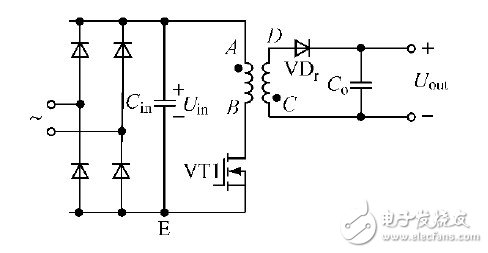
Take the flyback converter as an example, the main circuit is shown in Figure 1.
After the switch is turned on, the current on the primary side of the transformer gradually increases, and the energy storage of the core also increases. When the switch tube is turned off, the secondary side rectifier diode is turned on, and the transformer energy storage is coupled to the secondary side to supply power to the load.

Figure 1 flyback converter
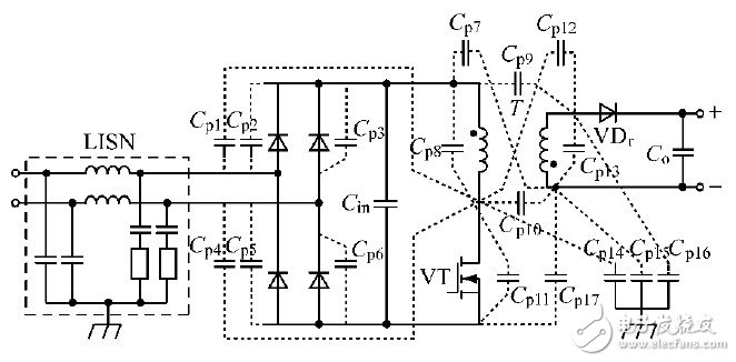
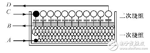
In the switching power supply, the input rectified current is a sharp pulse current, and the voltage and current change rates in the converter are high when the switch is turned on and off. These waveforms are rich in high frequency harmonics. In addition, during the main switch tube switching process and the reverse recovery process of the rectifier diode, the parasitic inductance and capacitance of the circuit will oscillate at a high frequency, and these are all sources of electromagnetic interference. There are a large number of distributed capacitors in the switching power supply. These distributed capacitors provide a path for the transmission of electromagnetic interference, as shown in Figure 2. In Figure 2, the LISN is a linear impedance-stabilized network for the measurement of line conducted interference. Interference signals are transmitted to the input and output terminals of the converter through wires, parasitic capacitances, etc., forming conductive interference. There is also a large amount of parasitic capacitance between the windings of the transformer, as shown in Figure 3. In Figure 3, points A, B, C, and D correspond to the four points identified in Figure 1.

Figure 2 Typical distribution of parasitic capacitance of a flyback switching power supply

Figure 3 Distribution of parasitic capacitance in a transformer
In the flyback switching power supply shown in Figure 1, when the converter is operating in continuous mode, after the switching transistor VT is turned on, the potential at point B is lower than point A, the primary winding inter-turn capacitance is charged, and the charging current flows from A to B; After VT is turned off, the parasitic capacitance is reversely charged, and the charging current flows from B to A. In this way, differential mode conducted EMI is generated in the transformer. At the same time, the potential difference between the power supply components and the ground also produces high frequency variations. Due to the distributed capacitance between the components and the earth and the casing, a common mode conducted EMI current flowing between the input terminal and the earth and the circuit formed by the casing is generated.
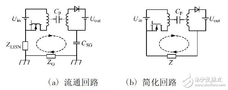
Specifically, in the transformer, the potential difference between the primary winding and the secondary winding also produces a high frequency variation, and the coupling of the parasitic capacitance produces a common mode conducted EMI current flowing between the primary side and the secondary side. The AC equivalent loop and the simplified equivalent loop are shown in Figure 4. In Figure 4: ZLISN is the equivalent impedance of the linear impedance stable network; CP is the parasitic capacitance between the primary winding and the secondary winding of the transformer; ZG is the equivalent impedance between different points of the earth; CSG is the equivalent between the output loop and the ground Capacitance; Z is the equivalent impedance of the circuit outside the transformer.

Figure 4 Flow circuit of common mode conducted EMI in a transformer
Cold And Heat Impact Test Chamber
Cold And Heat Impact Test Chamber,Thermal Shock Test Chamber,Cold And Heat Shock Test Machine,Climate Simulation Testing Test Box
Wuxi Juxingyao Trading Co., Ltd , https://www.juxingyao.com
