Radio frequency (RF) and microwave amplifiers provide optimum performance under specific bias conditions. The quiescent current determined by the bias point affects the performance performance indicators such as linearity and efficiency. While some amplifiers are self-biased, many devices require external biasing and use multiple power supplies whose timing needs to be properly controlled to make the device safe to operate.
Next, we mainly talk about the bias timing control requirements.
Power sequencing
Power sequencing is very important when using an external bias amplifier for the following reasons:
Failure to follow proper power sequencing can affect device stability. Exceeding the breakdown voltage may cause the device to fail immediately. Long-term reliability is reduced when conditions exceeding the boundary conditions occur multiple times and the system is under pressure. In addition, continuous violations of the timing control mode can damage the on-chip protection circuitry and cause long-term damage, resulting in field operation failures.
Optimizing the bias level during power-up and power-down, as well as during normal operation, can improve the performance of the RF amplifier, depending on configuration and application requirements. For some applications, the RF performance of the amplifier can be changed to suit different field conditions. For example, in rainy days, the output power can be increased to widen the coverage, and on a sunny day, the output power can be reduced. The amplifier's external gate voltage control enables these functions.
ADI has a wide range of RF amplifiers, many of which are based on depletion high electron mobility ( pHEMT ) technology. Transistors used in this process typically require a power supply to power the drain and gate pins. This quiescent drain current is related to the gate voltage.
See Figure 1 for typical IV characteristics of a typical field effect transistor (FET) process.
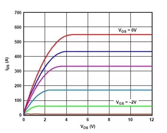
Figure 1. Typical IV characteristics of a typical FET process
As the gate-to-source voltage (VGS) increases, more electrons enter the channel, producing a higher drain-source current (IDS).
In addition, as the drain-source voltage (VDS) increases, the electric field force that pulls the electrons becomes larger, and the drain-source current also increases (in the linear interval).
In practical amplifiers, these amplifiers can be broadly classified into two categories due to effects such as channel length modulation: self-biased amplifiers and external bias amplifiers.
1 self-bias amplifierThe self-bias amplifier has an internal circuit to set the optimum bias point for operation. These amplifiers are typically best suited for broadband low power applications. See Figure 2 for a typical pinout of a self-biased amplifier.
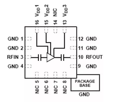
Figure 2. Typical pinout of a multistage self-biased amplifier with multiple bias pins
Self-biased amplifiers, while easy to use, may not provide optimal performance because internal resistive bias circuits do not adequately compensate for batch, device, and temperature differences.
2 external bias amplifierExternal bias amplifiers often provide higher performance than self-biased amplifiers under certain bias conditions. The quiescent drain current of the amplifier affects parameters such as power compression point, gain, noise figure, intermodulation products, and efficiency. For these high-performance external bias amplifiers, proper power sequencing is critical to ensure that the device operates safely at peak performance.
Figure 3 shows a typical connection of the external bias amplifier pins and the corresponding transistor pins. The pin mapping in Figure 3 is a simplified schematic of the amplifier.
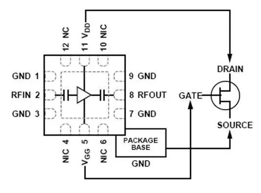
Figure 3. Typical connection of an external bias amplifier
In addition, many external bias amplifiers meet multiple gain, bandwidth, and power requirements through multiple stages. Figure 4 shows a typical block diagram of the multi-stage external bias amplifier HMC1131.
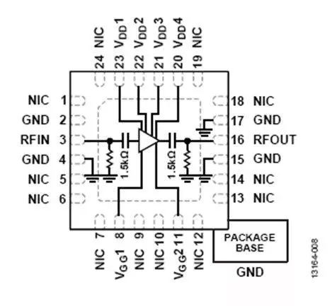
Figure 4. HMC1131 Multistage External Bias Amplifier
Give a chestnut: timing and control requirements for an external bias amplifier
The HMC1131 is a power amplifier for gallium arsenide (GaAs), pHEMT monolithic microwave integrated circuits (MMICs). The operating frequency range is from 24 GHz to 35 GHz. The typical performance offered by this 4-stage design is 22 dB gain, 23 dBm output power (1 dB compression, or P1dB) and 27 dBm saturated output power (PSAT). The corresponding bias conditions are VDD = 5 V and IDQ = 225 mA. Where VDD is the drain bias voltage and IDQ is the quiescent drain current. This information is given in the HMC1131 data sheet for the electrical specification table for the 24 GHz to 27 GHz frequency range. Figure 4 shows the pin connections for the HMC1131.
To achieve a target quiescent drain current (IDQ) of 225 mA, the gate bias pin voltages (VGG1 and VGG2) should be set between 0 V and −2 V. To set this negative voltage without damaging the amplifier, follow the recommended bias sequence during power-up and power-down.
The following is the recommended offset sequence during power-up of the HMC1131:
1
Connected to the ground
2
Set VGG1 and VGG2 to −2 V
3
Set the drain voltage bias pins VDD1 to VDD4 to 5 V
4
Increase VGG1 and VGG2 to achieve IDQ of 225 mA
5
Applying RF signal
The following is a recommended offset sequence during the HMC1131 power down:
1
Turn off the RF signal
2
Lower VGG1 and VGG2 to −2 V to achieve an IDQ of approximately 0 mA
3
Reduce VDD1 to VDD4 to 0 V
4
Increase VGG1 and VGG2 to 0 V
When the gate voltage (VGGx) is −2 V, the transistor is pinched off. Therefore, the typical value of IDQ is close to zero.
In general, the recommended bias sequences for most external bias amplifiers are similar. Different devices will have different IDQ, VDDx, and VGGx values. To turn off the device, VGG for GaAs devices is typically set to −2 V or −3 V, while for gallium nitride (GaN) amplifiers, this voltage can be −5 V to −8 V. Similarly, VDDx for GaN devices can reach 28 V or even 50 V, while GaAs amplifiers are typically less than 13 V.
The VGG pins of a multistage amplifier are typically tied together and biased together. Following the same procedure, the user can get the typical performance results available in the data sheet. Using an amplifier under different bias conditions may provide different performance. For example, using different VGGx levels for the HMC1131 gate bias pin to achieve different IDQ values ​​can change the RF and DC performance of the amplifier.
Figure 5 shows the P1dB vs. frequency for the HMC1131 at different supply currents. Figure 6 shows the output versus third-order intercept point (IP3) performance versus frequency for different supply currents.

Figure 5. P1dB vs. frequency for different supply currents
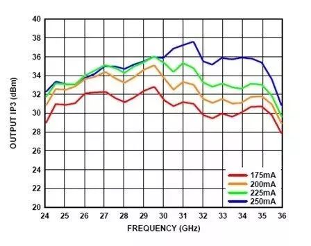
Figure 6. Output IP3 vs. frequency for different supply currents, POUT/sound = 10 dBm
Another option to utilize multiple VGGx pin bias amplifiers is to independently control the gate bias pins. This mode of operation helps the user customize the device by optimizing specific parameters such as P1dB, IP3, NF, gain, and power consumption.
This flexibility is beneficial for some applications. If the performance data provided in the amplifier data sheet can easily meet certain requirements of the application, but is slightly different from other requirements, test under different bias conditions without exceeding the absolute maximum ratings given in the data sheet. Performance may be beneficial.
Another alternative to biasing the external bias amplifier is to set VGGx to achieve the desired 225 mA IDQ and use a constant gate voltage during normal operation. In this case, the IDD of the amplifier will increase under RF drive (see the 30.5 GHz power compression diagram in the HMC1131 data sheet for this behavior). An amplifier with a constant gate voltage and an amplifier with a constant IDD may improve different performance.

Product catagories of stylus pen for ipad, which is just for iPad Versions 2018 & 2019 and above.
It can work on following:
iPad 6th 2018: A1893/A1954
iPad 7th 2019: A2197/A2198/A2200
iPad 8th 2020: A2270/A2428/A2429/A2430
iPad air 3rd: A2152/A2153/A2154/A2123
iPad Air 4th: A2072/A2316/A2324/2325
iPad mini 5th: A2124/A2125/A2126/A2133
iPad Pro 1st/2nd 11: A1980/A2013/A1934/A1979/A2228/A2068/A2230/A2231
iPad Pro 3rd/4th 12.9: A2069/A2229/A2233/A2232/A1876/A2014/A1895/A1983
Stylus Pen For Ipad,Stylus Pen,Stylus Pen For Drawing,Touch Pencil
Shenzhen Ruidian Technology CO., Ltd , https://www.szwisonen.com
