 How to reduce chip power consumption has become a hot issue in the semiconductor industry. In the past, the most straightforward approach for integrated device manufacturers (IDMs) was through advanced process technologies and materials such as low-k dielectrics, which can be achieved by combining the skills and experience of their design teams.
However, when entering 90nm, the leakage current problem has become increasingly prominent, and CMOS static power consumption has increased sharply, and power management has become an important consideration. This situation will be more serious at 65nm and below 45nm, because the continuous reduction of the process node leads to the thinner and thinner gate oxide layer, the gate leakage increases exponentially, and the final dynamic power consumption is equal to the subthreshold leakage current, which is equal to the gate. Extreme leakage current. This forces the industry to adopt low-power design techniques from the design side of the IC.
In response to these challenges, design engineers have begun to advocate complex clock gate switching schemes, thereby reducing unnecessary gate switching operations. Today, to meet power goals, designers use a variety of advanced low-power design techniques, including multi-threshold design, multi-voltage design, dynamic frequency voltage scaling (DVFS), clock gating, and memory-aware memory. Power gating and more.
Effective power evaluation early in the design processUndoubtedly, in terms of product success factors, time to market is one of the important factors, and sometimes even determines the success or failure of the product. Therefore, addressing potential low-power issues early in the design process is critical to increasing productivity.
Li An, a senior consultant engineer at Synopsys, said that the strategy and cost of evaluating low-power at the system level early in the design phase (ie, the system architecture phase) is very important for later implementations. The main considerations for low-power strategies evaluated at this stage include: partitioning of system hardware and software, whether to use multi-voltage (mulTI-voltage), whether to use power-off (mulTI-supply), on-chip or off-chip power management. , low power IP options, etc. At this stage of the evaluation, on the one hand, through the evaluation experience of the past system, on the one hand, through the rapid prototyping, the power estimation of the design prototype through the Eclypse system to evaluate the design cost and power saving effect.
Brad Miller, senior technical director at Cadence, also expressed the same view. He said that the following five aspects will ensure that designers achieve their goals efficiently and accurately: 1. Identify the components that consume power in the design; 2. Use accurate switching behavior data; 3. Consider the simulation mode when generating switching behavior; 4. Use a precise line model; 5. Use a library that represents the worst case power.

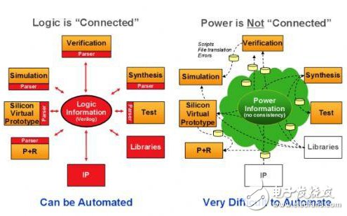
Figure 1: Many design relative logics are “connected,†but are “disconnected†to power consumption and do not automate the design.
Multiple low-power design solutions address power challengesHowever, EDA support for different low-power technologies is fragmented, and as a result designers have to define low-power features through a series of special means. More importantly, the predictability and verification of design becomes extremely difficult. At the same time, due to the complexity of the design and the lack of EDA automation, the engineering design team faced the challenge of manually analyzing and applying these techniques, and was not sure to meet the power budget goals without affecting performance.
Cadence related people pointed out that many of the current designs can be said to be "connected" to logic, because all processes process logical information and can be done automatically; but for power consumption is "disconnected" because for each Process, power consumption issues are independent and affect each other. And the most important thing is that power design can't be done automatically, and many places need to be done manually.
Therefore, effective low-power design requires collaboration between design teams, IP vendors, and tool and solution providers. Only by implementing a coherent approach and applying these methods to the entire tool domain in which the supply chain is based can the electronics industry truly address the growing challenges of low-power design.

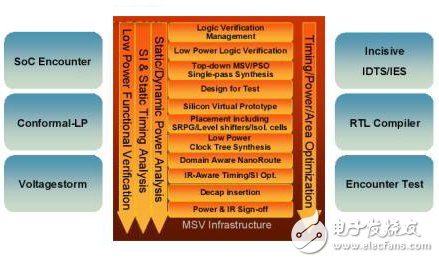
Figure 2: Synopsys Eclypse Low Power Solution
Synopsys Eclypse Low Power Solution
The Eclypse solution supports the standard Unified Power Format (UPF) language and is compatible with the Low Power Design Method Guide (LPMM). A variety of low-power design techniques such as MTCMOS power gating, multi-voltage, and dynamic voltage and frequency scaling (DVFS) have been used to make a major shift in engineer chip design and verification. Designers can take advantage of enhanced clock gating and low-power clock tree synthesis to optimize clock structures for low power while balancing clock jitter and timing; multi-threshold leakage current optimization options limit Vt ratios. Provides optimal leakage current power optimization independent of design processing; power switch insertion and optimized enhanced automation capabilities enable voltage drop and area limits for power planning and what-if analysis.
Cadence Low Power Design Methodology TipsCadence's Cadence Low-Power Methodology Kit provides an end-to-end methodology that covers logic design, functional verification, and physical implementation using Si2's Common Power Format (CPF). A single low-power intent specification is provided throughout the process. The kit includes a general-purpose wireless application design that uses multiple supply voltages and power-off techniques, and includes instruction scripts and technical documentation that carry design intent throughout the end-to-end process.
This kit is easy to use and includes six different processes: low power functional simulation, logic synthesis, testability design (DFT) and automatic test vector generation (ATPG), physical design, formal implementation, verification and work. Consuming grid signing. The user can implement the kit as a complete process or select a separate selection module to use.

Figure 3: Cadence Low-Power Design Methodology Tips
IC design low power standard disputeFrom the beginning of 2007, the two major EDA camps have launched fierce competition around the standards designed for low-power ICs. One is a CPF managed by Cadence, a low-power alliance (LPC) managed by Si2 (Silicon IntegraTIon IniTIative), and the other is UPF supported by Synopsys, Mentor Graphics, and Magma Design Automation. Both UPF and CPF allow users to define power design intents and constraints throughout the RTL-to-GDSII design flow, and the implementation of the two is very similar.
Julong, president of Cadence Asia Pacific, said that the advantage of CPF is that it is user-centric - user-driven, user-driven. The UPF standard is the response of the CPF. Initially, due to some patent issues, CPF was not placed in the public domain. But then Cadence submitted it to the IEEE, making CPF open to the industry. He believes that from a design perspective, there is absolutely no need to have two standards because they actually discuss the same thing.
Synopsys Bruce Jewett believes that UPF is an open language and its advantages are favored by IEEE. As for whether the two standards will be merged in the future, the two EDA giants all said that it depends entirely on market and commercial interests. In fact, users really care about having a certain solution that can help them solve the problems they are currently experiencing.
According to the Nikkei BP, the chief engineer of Renesas DFM and digital EDA technology department, Inoue Kazuo, questioned the fact that the two factions built the low-power design process by concentrating various specifications of EDA tools. He said: "If you use a lot of common common tools to build processes, there will be a mix of CPF and UPF tools. In this sense, the entire process of CPF and UPF is on paper."
But another interesting case is the introduction of ArchPro, which was called the "super combination" of wells called CPF and UPF, while supporting static verification and dynamic verification specifications, which was acquired by Synopsys in June 2007. In the Eclypse low-power solution launched by Synopsys, we have seen ArchPro tools such as MVRC and MVSIM. It is foreseeable that in the future, the camps of both sides will inevitably launch a fierce battle around low-power standards.
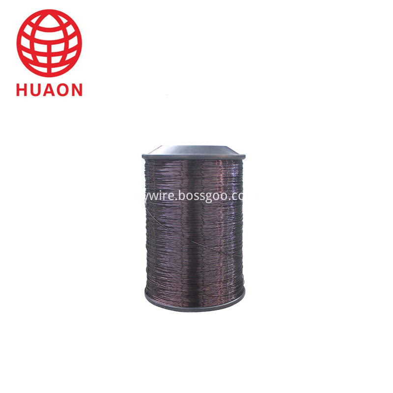
EI/ AIW Enameled Aluminium Wire
| About EI/ AIW Enameled Aluminium Wire |
Class 200 heavy insulation thickness of Polyester-imine / polyamide-imide compound enameled aluminum round wire

Product Name
Enameled aluminium wire EI/AIW
2065-6.00,CLASS C-200
Material
Aluminium
Type
EI/AIW
Themal class
calss C -200
Country of origin
China(Mainland)
Used
motor,transformer,rectifier and such
Enameled Aluminum Wire,Ei/ Aiw Enameled Aluminium Wire,Round Winding Wire,Super Enameled Aluminum Round Wire
HENAN HUAYANG ELECTRICAL TECHNOLOGY GROUP CO.,LTD , https://www.huaonwire.com
