In terms of its nature and history, the development of the electronic design industry is closely related to the progress of semiconductor device technology. With every advancement of technology on the basis of inheritance, when the potential of new device technology is fully developed, there will be real progress and innovation in product design. When some innovative engineering ideas touch the design tools, which not only provide new methods for using these technologies, but also can be designed in an unconstrained and easy-to-understand manner, this progress will occur.
Low-cost microprocessors were originally designed and conceived as a more efficient method of producing pocket calculators. As a result, its appearance has reflected the possibility of using software coding to enhance and increase product functionality. However, it is the innovative applications of new devices that use higher-level language tools because they allow the use of soft-design-centric approaches to design and achieve technological innovations. By exploring all design possibilities, engineers can transfer most of their hardware logic to changeable software domains. The full use of tools and technologies by engineering staff has prompted the functional “intelligence†that defines the value of products to begin to shift to the software domain.
At present, the emergence of low-cost, programmable high-intelligent devices such as FPGAs has brought another technological innovation to our design approach. These smart designs not only involve software in the traditional sense, but also include "soft" hardware implemented in an FPGA. Don't just use this technology as a glue logic reservoir as its basic potential, so that the unique features of the product and the resulting competitive advantages of the market can be defined in the modifiable software domain.
Designers of embedded systems now have a completely new design platform that can be used to create innovative products. When implementing a "soft" design approach using a fully configurable design platform, FPGAs bring unprecedented design freedom, thanks in part to a large number of available IP cores including logic blocks, peripherals and microprocessors . These can all be changed in accordance with the development of design requirements. Some key design decisions can be made later in the design cycle, while the hardware and software of the product can be updated in real time.
When the technology potential is fully utilized, the inherent "soft" design approach brings new freedom to the product development process. The desire to use this technology to create a product with true market differentiation means to overcome the many implementation issues that arise in the use of the technology. And this successful implementation is undoubtedly closely related to the innovation of the design tools we use.
Limitations introduced
In the traditional design flow, the design possibilities brought about by programmable devices are always accompanied by the increasing complexity of the entire product development process. A new level (or a new "realm") that has been introduced into the product development tool chain has traditionally been based on an embedded hardware development toolset that is independent of existing design processes and existing tools. The design process is irrelevant. When an independent FPGA-based component is integrated with the entire product design, this not only brings with it high complexity, but also requires you to master a new set of design skills to take full advantage of these embedded development tools.
The main reason for these challenges lies in the traditional series of IDE tools (integrated development environments) that originated in the ASIC design field, which uses HDL (hardware description language) to describe the hardware design of the pre-production chip. Using a traditional IDE tool chain means designing in a separate design environment and becoming an HDL expert while applying knowledge of these target FPGA infrastructures.
The most common situation is that the IDE is a tool chain owned by the FPGA device manufacturer. They are developed to support each vendor's products and promote sales, and naturally there is no support for competitive products. The use of a vendor IDE limits the inherent flexibility and freedom of embedded hardware design due to the limitations of the FPGA device's scope, the vendor's IP core, and the design methods you can use. In addition, if you want to change the programmable device used in your design, you'll have no alternative.
In practice, the limitations of the development tools themselves compromise the design choices that can be used in the pursuit of innovation.
Vendor-neutral design
To fully exploit the design possibilities of today's embedded design processes, you need a programmable device development environment that allows you to easily select multiple devices from different vendors. Creating a design environment completely independent of the vendor and the device opens the door to all the possibilities of the target, allowing the embedded developer to choose the best device for the current design.
Such a system is inherently neutral in an embedded design, allowing changes to the target device without compromising the validity of the design source file. In this way, you can make changes to the target device according to your own ideas, and make final decisions later in the design process when you can better understand the required specifications. The embedded design flow can be performed while all devices are still selected, without having to develop the hardware before the important embedded design begins.
A vendor-independent design system can also provide a broader range of IP cores because it enables you to achieve compatibility with the cores provided by the target vendor by making simple changes to the target device (such as a specific high-performance microprocessor). If you use the device-neutral framework in your system to develop an IP core library, the resulting hardware and software modules will show the same neutrality as the system. This brings to the eye-catching development prospect of using a neutral 32-bit microprocessor core in the initial development, and then changing the IP module to vendor-provided, with minimal impact on the completed design. The kernel.
The success of this approach depends in part on the availability of system upgrades that can be added with new device hardware support. You are free to use the latest programmable devices for your design with full system library IP core compatibility. At the same time, they also support the latest "soft" and discrete microprocessors and those embedded in the FPGA architecture because the system's embedded software tool chain has also been upgraded.
Designing in a truly vendor-neutral product development environment gives designers the freedom to easily explore all design possibilities. As the design progresses, we can fully choose to use programmable devices, microprocessors, and IP cores to create the most competitive products without any compromises.
Abstract transparency
The limitations of the traditional embedded design flow for device and IP range, and the mystery of HDL-based design capture (compared with assembly language for complex procedures) all require expert skills, and engineers cannot focus on innovative designs.
What is needed here is a system that enhances the abstraction of the design process so that design engineers can use and extend existing design skills, as well as design at a higher level. The potential benefit of high-level embedded design approaches is that hardware or software engineers can simply connect pre-verified IP blocks together in a way that is not only easy to achieve but also hides the underlying complexity of the device architecture.
By providing a schematic or diagram-based design interface, the embedded design process is improved without the need for expert HDL skills (though HDL inputs can be included). When such a system exists as a vendor-neutral embedded design environment, the process of replacing processors, peripheral devices, and memory may become a simple module-level operation through a graphical interface.
The main advantage of this system is that designers can fully focus on product development itself - functional "soft" intelligence. The high level of interface selection makes it easy to capture design intent without any complexity or other distracting interference.
When integrated into a system that natively supports common high-level design paradigms, the underlying hardware complexity is effectively hidden. Embedded hardware abstractions can include advanced IP interface systems (eg, Y-bus) and hardware interface IP cores that introduce transparent interconnect layers around processors, peripheral devices, and memory. By using a low-level interface architecture that supports reduced-complexity design interfaces, the embedded design actually becomes a “point by point†test.
Freedom through integration
Jumping out of traditional IDE-based design flows can provide engineers with valuable options based on existing options and provide innovative ways to create embedded designs. Manufacturers and device-independent embedded hardware design systems bring this all together and provide a high level of design abstraction. However, how the system connects with other parts of the design environment is also worth paying attention to.
In order to be fully effective, design abstraction and open device selection need to be reflected throughout the product development chain. In this way, the complex process brought by placing all design elements (hardware, software and programmable hardware) together in the traditional design becomes simple and transparent.
The integrated design system achieves this effect by placing all design domains in a single, consistent application. The design model becomes a single entity that runs through all domains, for example allowing the library IP module to contain multiple device support, graphics models, and hardware interface layers. Changes in the embedded design can be passed directly to the relevant domain using advanced automatic processes such as FPGA pin optimization. This becomes possible because all parts of the design process share the same single model of design data.
Applying an integrated vendor-independent design environment to the next phase of its logic means that those attributes are to be included in a joint hardware development platform. Hardware platforms that are vendor- and device-independent (possibly via plug-in FPGA board systems) and communicate directly with integrated applications can reflect the required flexibility and open design choices into the real world. Design iterations that require improvement and debugging of design projects can occur in real-time in real hardware, but also reduce the need for design simulation.
When this type of reconfigurable hardware platform is unified with the entire design system, from design capture to physical hardware, device and IP design choices made can be transparent throughout the entire design chain. In this way, the entire product development system becomes unified and coherent.
If the design environment also provides a high level of design abstraction, system developers will not be limited by the choice of devices and methods used to capture design intent. The ultimate result is an open approach to embedded system development that frees designers to focus on the design itself—creating functional device intelligence that provides true product differentiation.
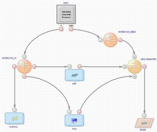
Figure 1: An advanced design capture system that automatically handles the underlying hardware complexity allows designers to focus on innovation.

Figure 2: In addition to the traditional HDL entry, suitable development tools can use the schematic-based capture or icon-based continuity control to abstract the embedded design to a higher level.
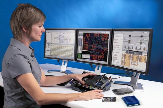
Figure 3: In an ideal design environment, all design systems, including hardware development platforms, can be unified within a single vendor-neutral product development system.

Figure 4: A design system that does not depend on FPGA devices and can provide an advanced design abstraction can provide all the options needed to create a competitive product without making any compromises.
The most comprehensive introduction of LED PCB
The relationship between LED and PCB
The Printed Circuit Board is a genius innovation of circuit technology, laying less space and materials for more complex and large-scale circuits. The printed circuit board is such an important invention in circuit technology because it makes electrical and electronic components smaller, more flexible and more precise. For example, FPC( Flexible PCB ), Multilayer PCB , BGA PCB , rigid- Flex PCB and so on.
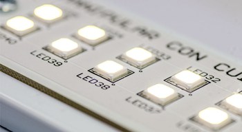
Soldering the LED chip to the PCB Board , as long as the PCB circuit is connected in some way, it will illuminate, which forms the LED PCB. LED PCBs typically also have a heat sink and ceramic pedestal to hold the circuit in place and allow the smooth operation of the circuit. A heat sink is required because LEDs tend to generate a lot of heat, which can damage the PCB and the equipment that connects the circuits.
Because LED will produce a lot of heat, led PCB generally uses metal substrate as its production material. Metals with the ability to dissipate heat quickly have proved to be a better choice. Generally, whenever led PCB is designed, Aluminum PCB is preferred. Aluminum PCB usually also contains a thin layer of dielectric, which can dissipate heat faster.
In addition to general lighting, led PCB can also provide visible light, infrared and ultraviolet light. Compared with other light sources, LED PCB can provide higher energy.
We are a professional LED PCB manufacturer and assembler in China, In this article, we would like to introduce in detail what is LED PCB, the materials used in manufacturing and LED circuit boards manufacturing, the application of LED Printed Circuit Boards and so on.
In China, there are many PCB manufacturers and suppliers. Jinghongyi PCB is one of the LED PCB Board manufacturers. We only provide LED PCB fabrication services. LED PCB design is not our specialty and business scope.
LED PCB board Introduction
LED PCB has many other names, such as LED PCB board, LED circuit, LED Circuit Board, led printed circuit boards, PCB board for LED.
In a sense, LED PCB and aluminum PCB belong to the same kind of PCB products, because their uses and materials are mostly the same.
With the popularization and widespread use of industrial lighting and civil lighting, whether outdoor or indoor, family or commercial buildings and factories, lighting provides the guarantee of its normal operation.
Of course, nowadays, with the development of human society, environmental pollution has become a difficult problem in the world. In order to reduce the consumption of coal, such as coal used for power generation in thermal power plants, coal combustion pollutes the atmosphere very seriously. In order to save energy and protect the environment, LED lights and previous lighting methods have great advantages, except for energy. Besides providing brighter lights, it also contributes to environmental protection.
LED PCB Meaning
LED circuit board is a kind of printed circuit board.

LED PCB Board manufactureing
Both LED aluminium PCB and FR-4 fiberglass circuit board belong to PCB. To say differently, only compare LED aluminium substrate with FR-4 fiberglass circuit board.
LED aluminium substrate is printed on the surface of aluminium material with better thermal conductivity, and then weld electronic components on it.
In electronics, an LED circuit or LED driver is an electrical circuit used to power a light-emitting diode (LED). The circuit must provide sufficient current to light the LED at the required brightness, but must limit the current to prevent damaging the LED.
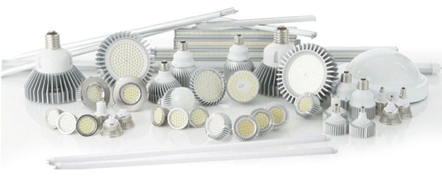
The voltage drop across an LED is approximately constant over a wide range of operating current; therefore, a small increase in applied voltage greatly increases the current.
Very simple circuits are used for low-power indicator LEDs. More complex, current source circuits are required when driving high-power LEDs for illumination to achieve correct current regulation.
An LED PCB board tends to generate a high volume of heat, making it difficult to cool via traditional means.
LED PCB Board Material - LED PCB raw material, LED bulb PCB raw material, LED strip PCB material
Metal core PCBs are often chosen for LED applications because they have enhanced heat dissipation capabilities. In particular, aluminium is usually used to make circuit boards for LED lamps. Aluminum substrates usually consist of thin layers of thermal conductive dielectrics that can be transported and have much more efficient heat dissipation than conventional rigid PCBs.
Compared with other electronic components, LED generates more heat, which requires PCB to heat very well. For this special feature, Metal Core PCB is often used in LED circuit boards, especially Aluminum Core PCB .
The following is the heat dissipation capacity of PCB plates of different materials, from weak to strong
1. FR4, common PCB board material;
2. Alumina substrate;
3. There is no doubt that the thermal conductivity of ceramic PCB is the best among many materials;
4. The thermal conductivity of alumina ceramic circuit board can be about ten times that of the aluminum substrate;
5. The thermal conductivity of Slyton aluminum nitride ceramic circuit board is ten times higher than that of alumina;
In this kind of ultra-high thermal conductivity, LED light attenuation will be greatly weakened, and its service life will be greatly increased.
LED Lighting PCB Assembly
Seeking LED PCB and Assembly? LED PCB Manufacturing and assembly; Led board made based on your PCB files. Turn-key services; 100% inspection.
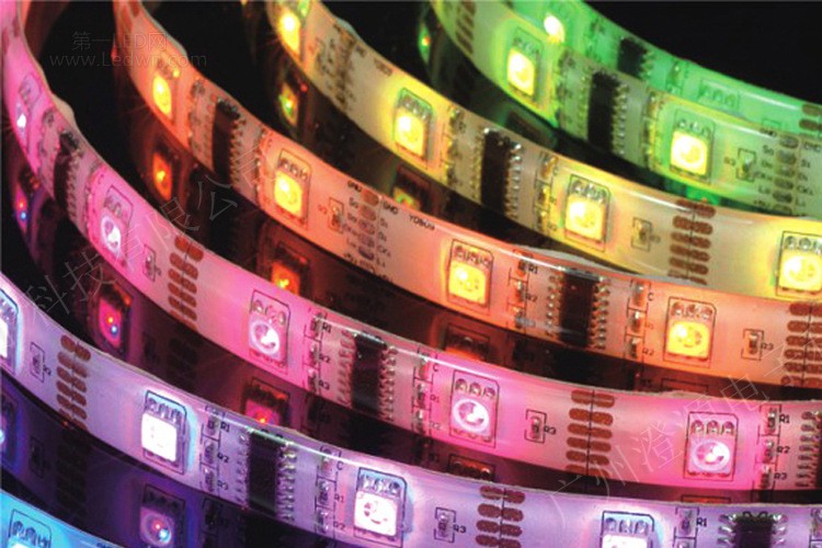
Applications of LED PCB
PCB LED lights can be incorporated into numerous lighting applications due to their combination of excellent energy efficiency, low cost and maximum design flexibility.
- Automotive headlights
- Airport runway landing lights
- Lighting used in military field
- Street lighting
- Highway tunnel lighting
- Photovoltaic (solar) lighting
- Flashlights and lanterns
- Traffic and signal lighting
- Lighting in hospital operating rooms
- High growth plant lighting
- Highway tunnel lighting
- Solar power products
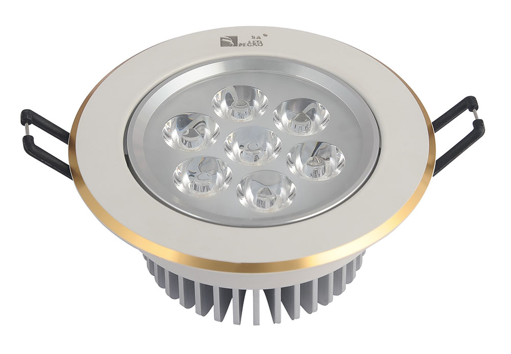
If you have any questions about LED PCB Board, Please feel free to send us email. If you have final Gerber for production, welcome your inquiry.
Additional Information
Aluminum PCB for LED Light/Lamp/Tube
Aluminum PCB for LED
Aluminium Base LED PCB
LED Metal Core PCB
Metal Core PCB for LED
PCB industry cut into LED PCB heat sink aluminum substrate
Double Sided Aluminum PCB
LED PCB
LED PCB,LED Circuit Board,LED PCB Board,LED Printed Circuit Board
JingHongYi PCB (HK) Co., Limited , https://www.pcbjhy.com
