
1 Introduction
TL431 is a three-terminal adjustable precision voltage reference integrated chip with good thermal stability. It has the characteristics of small size, low price and excellent performance. Its output voltage can be arbitrarily set to the reference voltage with two resistors (2.5). V) Any value in the range of 36V, typical dynamic impedance is only 0.2Ω, voltage reference error is ±0.4%, load current capability is from 1.0mA to 100mA, temperature drift is low, output noise voltage is low. Based on the above characteristics, it can be used not only in constant current source circuits, voltage comparator circuits, voltage monitor circuits, overvoltage protection circuits, etc., but also widely used in linear regulated power supplies such as linear regulated power supplies and switching regulated power supplies. In this paper, the TL431 parallel and series power supplies in linear regulated power supply are introduced in detail.
2. Internal structure and function of TL431
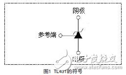
2.1 Symbols of TL431
The symbol of the device is shown in Figure 1. The three pins are: cathode (CATHODE), anode (ANODE) ​​and reference terminal (REF), and the reference voltage is 2.5V.
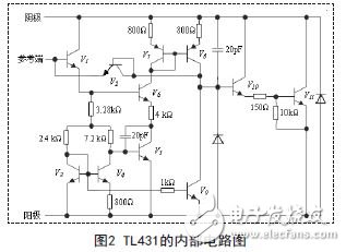
2.2 Internal Circuit Diagram of TL431
It can be seen from the internal circuit diagram 2 that it consists of a multi-pole amplifier circuit, a bias circuit, a compensation and protection circuit, in which the transistor V1 constitutes an input pole, V3, V4, V5 form a voltage regulation reference, and the mirror images of V7 and V8 are constant. The flow source and V6 and V9 form a differential amplifier for the intermediate stage, and V10 and V11 form a composite tube to form an output. Other resistors, capacitors, and diodes respectively function as offset, compensation, and protection. In principle, it is a single-ended. Input, single-ended output DC amplifier.
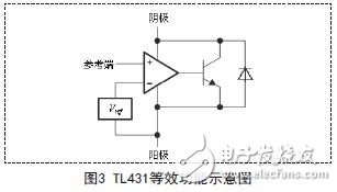
However, its equivalent function diagram is shown in Figure 3. It consists of a 2.5V precision reference voltage source, a voltage comparator and an output switching transistor. The output voltage of the reference terminal is compared with the precision reference voltage source Vref. When the voltage exceeds 2.5V, the TL431 turns on immediately. Since the R terminal control voltage error is ±1%, the reference terminal can accurately control the turn-on and turn-off of the TL431.
3. Parallel voltage regulator circuit design
3.1 Basic shunt regulator circuit principle
The TL431 contains a 2.5V reference internally, so when the output feedback is introduced at the Vref terminal, the device can control the output voltage by a wide range of shunts from the cathode to the anode. As shown in the circuit of Figure 4, when the resistance values ​​of R1 and R2 are determined, the two introduce feedback on the partial pressure of VO. If the feedback amount increases, the shunt of TL431 increases, which in turn causes VO to drop. Obviously, this deep negative feedback circuit must be stable at the same reference voltage. At this time, VO=(1+R1/R2)Vref. Selecting different values ​​of R1 and R2 can get any voltage output from 2.5V to 36V. In particular, when R1=R2, VO=5V. If R1 is short-circuited, R2 is open, that is, the reference terminal and the cathode terminal are short-circuited. At this time, there is output voltage VO=2.5V (reference terminal voltage), which is most suitable. Used as a reference voltage source in digital voltmeters and analog-to-digital converters or other circuits.
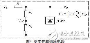
It should be noted that the necessary condition for ensuring the operation of the TL431 when selecting the resistor R is that the current through the cathode is greater than 1 mA, and R1 and R2 should select the same type of resistor with an accuracy of 1% to ensure the long-term stability of the reference power supply.
Solar Power System Accessories
Solar Power System Accessories,Solar System Accessories,Solar Installation Kit,Solar Battery Kit
SUZHOU DEVELPOWER ENERGY EQUIPMENT CO.,LTD , https://www.fisoph-power.com