The Cortex-M is Atmel's new Atmel SAM D20 microcontroller, which is based on a global microcontroller standard.
Cortex-M processor familyThe Cortex-M processor family is more focused on the lower performance side, but these processors are still very powerful compared to the traditional processors used by many microcontrollers. For example, the Cortex-M4 and Cortex-M7 processors are used in many high-performance microcontroller products with a maximum clock frequency of 400 MHz.
Of course, performance is not the only indicator for selecting a processor. In many applications, low power consumption and cost are the key choices. Therefore, the Cortex-M processor family includes a variety of products to meet different needs:
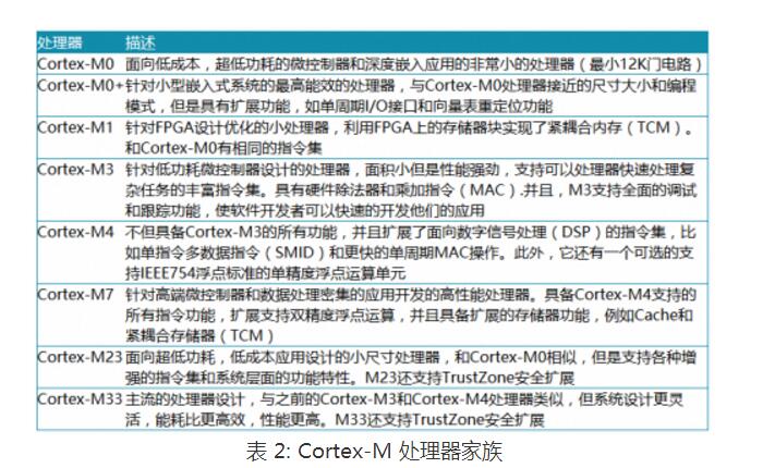
There are many similarities between Cortex-M0, M0+, M3, M4 and M7. For example:
- Basic programming model
- Interrupt Response Management of Nested Vectored Interrupt Controller (NVIC)
- Architecture-designed sleep modes: sleep mode and deep sleep mode
- Operating system support features
- Debugging function
- Ease of use
For example, a nested vectored interrupt controller is a built-in interrupt controller
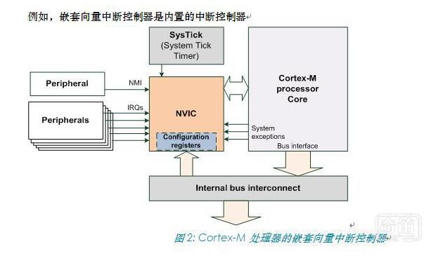
Supports many peripheral interrupt inputs, a non-maskable interrupt request, an interrupt request from the built-in clock (SysTIck), and a number of system exception requests. The NVIC handles the priority and mask management of these interrupts and exceptions.
More information on NVIC and the exception handling model is described in Section 3.2. The similarities and differences between other Cortex-M processors will be explained in the rest of this article.
Cortex-M Series Processor Architecture Features1, programming model
The programming model of the Cortex-M processor family is highly consistent. For example, all Crotex-M processors support R0 through R15, PSR, CONTROL, and PRIMASK. Two special registers - FAULTMASK and BASEPRI - supported only by Cortex-M3, Cortex-M4, Cortex-M7, and Cortex-M33; floating-point register set and FPSCR (Floating-Point Status and Control Register) register, Cortex-M4/M7 /M33 Optional floating-point unit.
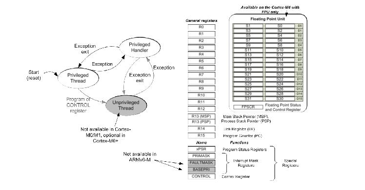
Figure 5: Programming Model
The BASEPRI register allows programs to block specified or low priority interrupts and exceptions. This is important for ARMv7-M because Cortex-M3, Cortex-M4, Cortex-M7, and Cortex-M33 have a large number of priority levels, while ARMv6-M and ARMv8-M Baseline have only a limited four priorities. grade. FAULTMASK is usually used for complex error handling (see section 3.4)
Non-privilege level implementations are optional for ARMv6-M processors and are always supported on ARMv7-M and ARMv8-M processors. For the Cortex-M0+ processor, it is optional and Cortex-M0 and Cortex-M1 do not support this feature. This means that the CONTROL registers on various Cortex-M processors are slightly different. The FPU configuration also affects the CONTROL register, as shown in Figure 6.
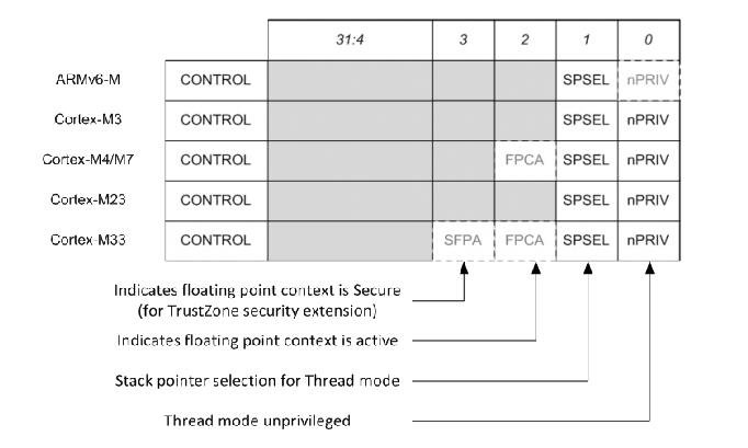
Fig. 6: CONTROL register
The difference between the other programming models is the details of the PSR register (program status register). For all Cortex-M processors, the PSR register is subdivided into the Application Status Register (APSR), the Program Status Register (EPSR), and the Interrupt Program Status Register (IPSR). ARMv6-M and ARMv8-M Baseline series processors do not support the QSR of the APSR and the ICI/IT bit of the EPSR. The ARMv7E-M series (Cortex-M4, Cortex-M7) and ARMv8-M Mainline (Cortex-M33 with DSP extensions) support the GE bit. In addition, the number range of the interrupt number of the ARMv6-M series processor IPSR is very small, as shown in Figure 7.

Figure 7: PSR Differences
Please note that the Cortex-M programming model and ARM7TDMI are not the same as these classic ARM processors. The definition of "mode" and "state" in the classic ARM processor is different from that in the Cortex-M except for the register set. Cortex-M has only two modes: Thread and Handler, and the Cortex-M processor is always in Thumb state (ARM instructions are not supported).
2, exception handling model and nested vector interrupt controller NVIC
All Cortex-M processors include the NVIC module and use the same exception handling model. If an abortion occurs, its priority is higher than the current run level, and it is not masked by any interrupt mask register. The processor will respond to this interrupt/exception and push some registers onto the current stack. With this type of stacking mechanism, interrupt handlers can be written as a normal C function. Many small interrupt handlers can immediately respond directly to work without the extra stack processing overhead.
The interrupts and system exceptions used by some ARMv7-M/ARMv8-M Mainline series processors are not supported by ARMv6-M/ARMv8-M Baseline products, as shown in Figure 8. For example, the number of interrupts for Cortex-M0, M0+, and M1 It is limited to 32 or less, there is no debug monitoring exception, and the error exception is also limited to HardFault (for details of error handling, see section 3.4). In contrast, Cortex-M23, Cortex-M3, Cortex-M4 and Cortex-M7 processors can support up to 240 peripheral interrupts. The Cortex-M33 supports up to 480 interrupts.
Another difference is the number of priority levels that can be used:
ARMv6-M Architecture - ARMv6-M supports two fixed (NMI and HardFault) and four programmable (represented by two bits per priority register) interrupt/abort priority. This is sufficient for most microcontroller applications.
ARMv7-M architecture - ARMv7-M series processors have a programmable range of priority levels, which can be configured from 8 levels (3 bits) to 256 levels (8 bits) depending on the area. The ARMv7-M processor also has a function called interrupt priority grouping, which can further divide the interrupt priority register into group priorities and sub-priorities, which can specify preemptive priority behavior in detail.
ARMv8-M Baseline – Like ARMv6-M, M23 also has a 2-bit priority level register. With the optional TrustZone security extension component, security software can shift the priority of interrupts in non-secure environments to the lower half of the priority range, which ensures that certain interruptions/abnormalities in the security environment are always less secure than non-security. The priority in the environment is higher.
ARMv8-M Mainline - Similar to ARMv7-M. Eight to 256 interrupt priority levels and interrupt priority groups can be supported. Also supports the ARMv8-M Baseline priority adjustment feature.
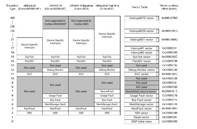
Figure 8: Cortex-M processor exception interrupt type
All Cortex-M processors rely on vector tables for exception handling. The vector table holds the starting address of the exception handler (as shown in Figure 8). The starting address of the vector table is determined by a vector table offset register (VTOR).
Cortex-M0+, Cortex-M3 and Cortex-M4 processors: by default the vector table is located in the starTIng of the memory map (address 0x0). Cortex-M0+, Cortex-M3 and Cortex-M4: The vector table defaults to the starting address of the memory space (address 0x0).
Cortex-M23 and Cortex-M33 processors can have two separated vector tables for Secure and Non-secure excepTIons/interrupts. Cortex-M7, Cortex-M23 and Cortex-M33: The initial value of VTOR is defined by the chip designer. The Cortex-M23 and Cortex-M33 processors have two independent vector tables for safe and non-secure exceptions/interrupts.
Cortex-M0 and Cortex-M1 does not implement a programmable VTOR and vector table starTIng address is always 0x00000000. Cortex-M0 and Cortex-M1 do not implement a programmable VTOR. The vector table start address is always 0x00000000.
The VTOR for Cortex-M0+ and Cortex-M23 processors is optional. If VTOR is implemented, the starting address of the vector table can be changed by setting VTOR. This function is useful for the following situations:
Relocate vector table to SRAM to dynamically change exception handler entry point
Relocate vector table to SRAM for faster vector read (if flash memory is slow)
Relocate vector table to ROM in different locations (or Flash). Different program execution phases can have different exception handlers
There are additional differences in the NVIC programming model between different Cortex-M processors. The differences are summarized in Table 5:
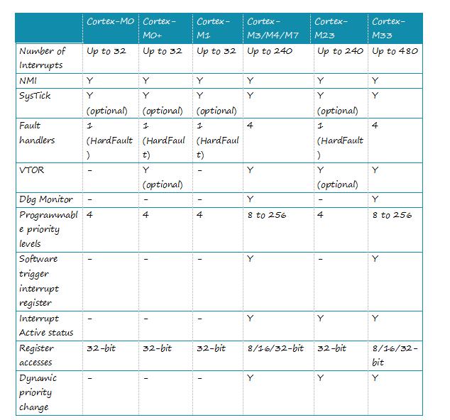
Table 5: Differences in NVIC Programming Models and Features
In most cases, the operations of the NVIC's interrupt control features are handled through APIs provided by CMSIS-CORE. They are in the device driver library provided by the microcontroller manufacturer. For the Cortex-M3/M4/M7/M23/M33 processor, its priority can be changed even if the interrupt is enabled. The ARMv6-M processor does not support dynamic priority adjustment. When you need to change the interrupt priority level, you need to temporarily turn off the interrupt.
3, operating system support features
The Cortex-M processor architecture is designed with operating system support in mind. The characteristics of the operating system are:
Shadow stack pointer
System Service Call (SVC) and Suspendable System Call (PenSV) exceptions
SysTick – 24-bit countdown timer that generates periodic exceptions for timing and task management of the operating system
Unprivileged Execution and Storage Protection Unit (MPU) Supported by Cortex-M0+/M3/M4/M7/M23/M33
A system service call (SVC) exception is triggered by an SVC instruction, which allows an application running in an unprivileged state to start a privileged operating system service. Suspending System Call Exceptions Scheduling non-critical operations such as context switching in the operating system is very helpful.
In order to be able to place the Cortex-M1 in a small FPGA device, all features used to support the operating system are optional for the Cortex-M1. For the Cortex-M0, Cortex-M0+ and Cortex-M23 processors, the system clock SysTick is optional.
In general, all Cortex-M processors support the operating system. Implementations on Cortex-M0+, Cortex-M3, Cortex-M4, Cortex-M7, Cortex-M23, and Cortex-M33 applications can run in unprivileged operating state and can use optional memory management units (MPUs) at the same time to avoid Invalid memory access. This can enhance the robustness of the system.
4, TrustZone security extension
In recent years, the Internet of Things (IoT) has become a hot topic for embedded system developers. IoT system products have become more complex and the pressure of time to market has also increased. Embedded system products need a better solution to ensure the security of the system, but at the same time it is easier for software developers to develop. The traditional solution is to divide the software into two parts: privileged and non-privileged. The privileged software uses MPU to prevent non-privileged applications from accessing critical system resources including security-sensitive information. This scheme is suitable for some IoT systems, but in some cases, only two layers are not enough. Especially for systems that contain many software components with complex privilege levels, a flaw in privileged code can lead hackers to completely control the system.
The ARMv8-M architecture includes a security extension called TrustZone, which imports orthogonal partitions of both secure and non-secure states.
Normal application is non-secure
Software components and security-related resources (eg, secure storage, cryptographic accelerators, TRNG) are in a secure state.
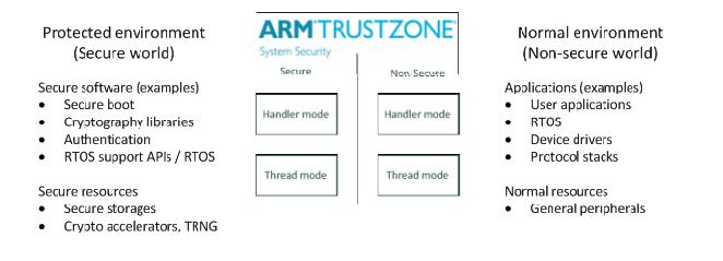
Figure 9: Isolation between safe and non-secure states
Non-secure software can only access non-secure storage space and peripheral devices. Security software can access all resources under both conditions.
With this approach, software developers can use the past to develop applications in non-secure environments. At the same time, they can use the secure communication software library provided by the chip manufacturer to implement the secure IoT connection. And even if there are loopholes in privileged programs that run in non-secure environments, the TrustZone security mechanism can prevent hackers from controlling the entire device, limiting the impact of the attack, and enabling remote system recovery. In addition, the ARMv8-M architecture also introduces stack boundary checking and enhanced MPU design, facilitating the adoption of additional security measures.
The security architecture definition also extends to the system level, and each interrupt can be set to security or non-security attributes. The interrupt exception handler also automatically saves and restores register data in the secure environment to prevent leakage of security information. Therefore, the TrustZone security extension allows the system to support real-time system requirements, provides a solid security foundation for IoT applications, and allows software development to develop applications on this technology.
The TrustZone module is optional for the Cortex-M23 and Cortex-M33 processors. For more information on the ARMv8-M TrustZone, look for The Next Steps in the Evolution of Embedded Processors for the Smart Connected Era. For more TrustZone resources, please see "TrustZone for ARMv8-M Community" on community.arm.com
System characteristics1, low power consumption
Low power consumption is a key advantage of the Cortex-M processor. Low power consumption is an integral part of its architecture:
• WFI and WFE instructions
• Architecture-level sleep mode definitions
In addition, Cortex-M supports many other low-power features:
• Sleep and Deep Sleep modes: The features supported by the architecture level can be further extended with device-specific power management registers.
• Sleep-on-exit mode: Low-power technology for interrupt-driven applications. After the setting is turned on, the processor automatically enters sleep mode when the exception handler ends and there is no other interrupt pending. This avoids the execution of instructions in the extra thread mode to save power, and reduces unnecessary stack read and write operations.
• Wake-up interrupt controller (WIC): An optional feature that detects interrupt conditions from a small, processor-independent module in a specific low-power state. For example, in a state-retention power management (SRPG) design, the design is when the processor is powered off.
• Clock off and architecture-level clock off: Power is saved by turning off the processor's registers or sub-module clock inputs
All these features are supported by Cortex-M0, Cortex-M0+, Cortex-M3, Cortex-M4, Cortex-M7, Cortex-M23 and Cortex-M33. In addition, various low-power design techniques are used to reduce processor power consumption.
Cortex-M0 and Cortex-M0+ processors consume less power than Cortex-M3, Cortex-M4 and Cortex-M7 because of fewer circuits. In addition, the Cortex-M0+ extra optimization reduces program access (eg, jump backups) to maintain system-level low power consumption.
Cortex-M23 is not as small as Cortex-M0 and Cortex-M0+, but it is still the same as Cortex-M0+ in the same configuration.
Due to better performance and low power optimization, the Cortex-M33 has better power efficiency than the Cortex-M4 under the same configuration.
2, Bit-band feature bit segment
The Cortex-M3 and Cortex-M4 processors support an optional feature called bit-segment that allows two segments of bit-addressable 1MB of address space with bit-segment alias addresses (a segment of SRAM starting at address 0x20000000 The other segment is the peripheral space starting at address 0x40000000). Cortex-M0, M0+, and Cortex-M1 do not support bit-band functionality, but bit-band functionality can be implemented at the system level using bus level components in the ARM Cortex-M System Design Suite (CMSDK). . Cortex-M7 does not support bit-band, because M7's Cache function cannot be used in conjunction with bit-segment (the cache controller does not know the alias address of the memory space).
The ARMv8-M's TrustZone does not support bit segments because the two different addresses required by the segment alias may be in different security domains. For these systems, bit manipulation of peripheral data can instead be handled at the peripheral level (for example, by adding bit settings and clearing registers).
3, memory protection unit (MPU)
In addition to Cortex-M0, other Cortex-M processors have optional MPUs to implement the definition of storage space access rights and storage space attributes or storage intervals. In an embedded system running a real-time operating system, the operating system defines the storage space access permissions and memory space configuration for each task to ensure that each task does not destroy other tasks or the address space of the operating system kernel. The Cortex-M0+, Cortex-M3 and Cortex-M4 all have 8 programmable area spaces and a very similar programming model. The main difference is that the Cortex-M3/M4 MPU allows two levels of storage space attributes (for example, system-level cache types), and the Cortex-M0+ only supports one level. The Cortex-M7 MPU can be configured to support 8 or 16 zones with two levels of storage space attributes. Cortex-M0 and Cortex-M1 do not support MPU.
The Cortex-M23 and Cortex-M33 also support the MPU option, which can have up to two MPUs if the TrustZone security extension is implemented (one for secure software programs and one for non-secure software programs).
Single-cycle I/O interface
The single-cycle I/O interface is a unique feature of the Cortex-M0+ processor, which allows the Cortex-M0+ to quickly run I/O control tasks. The bus interface of most Cortex-M processors is based on the AHB Lite or AHB 5 protocol. These interfaces are pipelined bus protocols that operate at high clock frequencies. However, this means that each transfer takes two clock cycles. The single clock cycle I/O interface adds an extra simple, non-pipelined bus interface to a subset of device-specific peripherals like GPIO (General Purpose Input Output). Combining the natural low latency of single-cycle I/O and Cortex-M0+ (only two pipeline stages), many I/O control operations will run faster than most other microcontroller architecture products.
Debugging and tracing featuresThere are several differences between different Cortex-M processors. Summarized in Table 9.
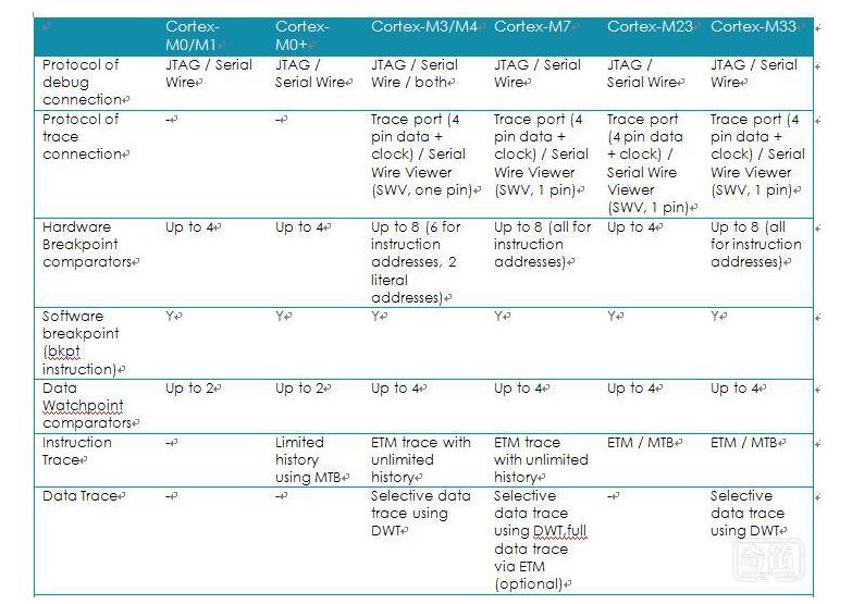
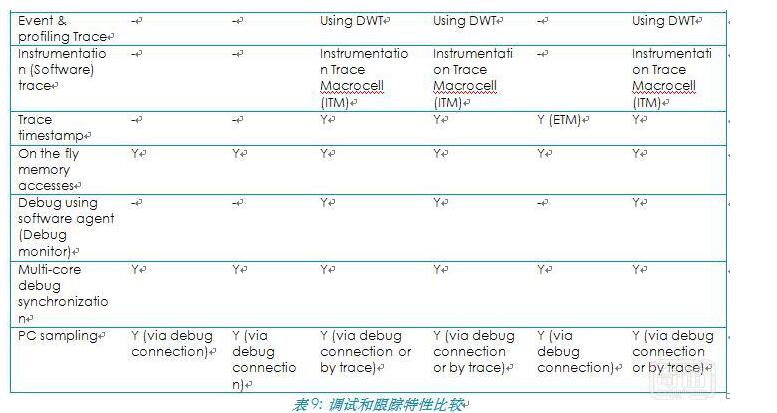
The Cortex-M processor's debug architecture is based on the ARM CoreSight debug architecture. It is an extremely scalable architecture that supports multiprocessor systems.
Table 9 lists the typical designs that need to be considered. Under the CoreSight architecture, the debug interface and trace interface module are separate from the processor. Therefore, the debug and trace connection of the equipment you use may not be the same as in Table 9. It is also possible to add some debugging features by adding some additional CoreSight debugging components.
6.2 Debug connections debug interface
Debugging interface allows debuggers to implement
- Access registers that control debug and trace features.
- Access to memory space. For Cortex-M series processors, memory space access can also be performed in time when the processor is running. This is called real-time memory access.
- Access to processor core registers. This can only be operated when the processor is stopped.
- Access trace history generated by the Micro Trace Cache (MTB) in the Cortex-M0 processor.
In addition, the debug interface is also used as:
- Flash programming
Cortex-M series processors can select the traditional 4 to 5 pin (TDI, TDO, TCK, TMS, and optional nTRST) JTAG interface, or select a new serial debugging protocol interface that requires only two pins The serial debug interface is well suited for a limited number of pin devices.
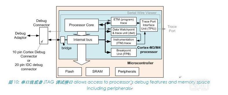
The serial line debug protocol interface handles all the features supported by JTAG and supports parity checking. The serial debugging protocol is widely used by ARM tool manufacturers. Many debug adapters support both protocols. Serial cable models share the TCK and TMS pins on the debug interface.
6.3 Trace Interface
The trace interface allows the debugger to collect information about the program's operation in real-time (very small delays) when the program is executed. The collected information can be the program instruction stream information (instruction trace) generated by the Cortex-M3/M4/M7/M33 supported embedded trace unit (ETM), which can be data/event/performance analysis generated by the data tracking unit (DWT). Information, or information generated by the software control data tracking unit (ITM).
There are two types of trace interfaces available:
- Trace port - Multiple data lines plus clock signal lines. The higher tracking bandwidth than SWV can support all trace types of SWV plus instruction tracking. On Cortex-M3/M4/M7 or Cortex-M33 devices, the trace port usually has 4 data lines and a clock line. (Figure 11)
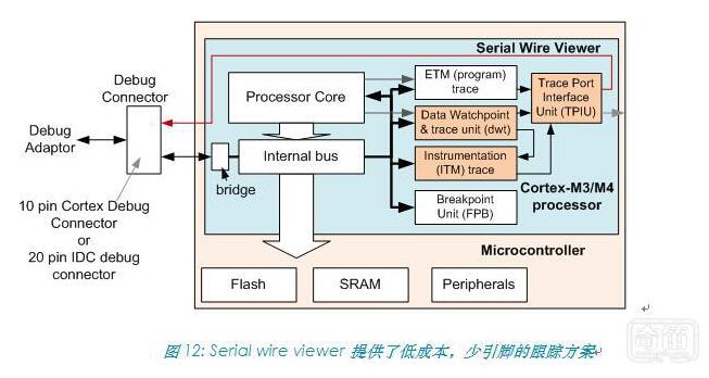
- Serial Monitor (SWV) – A single-lead line trace interface that can optionally support data tracking, event tracking, performance analysis, and measurement tracking. (Figure 12)
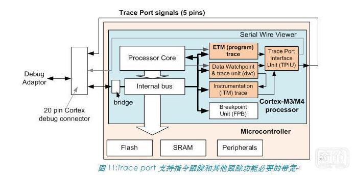
The trace interface provides the ability to get a lot of useful information while the processor is running. For example, the embedded tracking unit (ETM) can acquire the instruction running history, and the data tracking unit (ITM) allows the software to generate a message (for example, via printf) and acquire it using the Trace interface. In addition, the Cortex-M3/M4/M7/M33 supports Data Tracking Unit (DWT) modules.
- Optional data tracking: information on the memory address (for example, address, data, and timestamp combinations) can be collected when the processor accesses this address
- Performance analysis tracking: The number of clock cycles used by the CPU in different operational tasks (for example, memory access, sleep)
- Event Tracking: Provides interrupt/abnormal run time and history of server response
These tracking features are widely used by various tool manufacturers, and the collected information is also displayed in various ways. For example, the data obtained by the DWT can be displayed in a waveform in the Keil μVision debugger (part of the Keil microcontroller development tool) as shown in Figure 13.
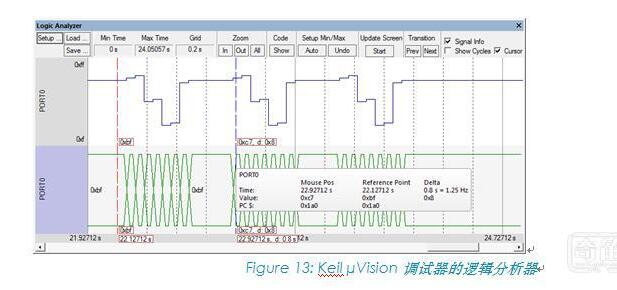
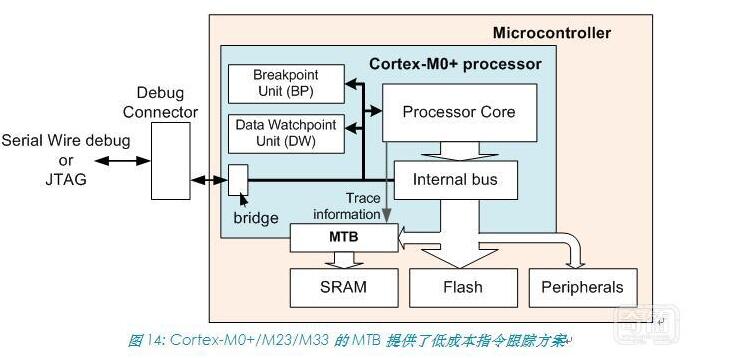
Although the Cortex-M0 and Cortex-M0+ do not support the trace interface, the Cortex-M0+ supports a feature called Micro Trace Cache (MTB, Figure 14). MTB allows the user to allocate a small piece of system SRAM as a cache for storing instructions, usually set as a circular buffer, so that the latest instruction execution history can be captured and displayed on the debugger.
This MTB tracking feature is also supported by Cortex-M23 and Cortex-M33.
There is always a balance between performance, characteristics and chip area, and power consumption. To this end, ARM has developed various Cortex-M processors with different levels of instruction set features, performance, system, and debugging features. This article describes the differences and similarities of the Cortex-M processor family.
Despite this difference, the consistency of the architecture and the CMSIS-CORE standardized APIs all make the Cortex-M series processor software more portable and reusable. At the same time, Cortex-M series processors are very convenient to use. As a result, the Cortex-M family of processors quickly became the most popular 32-bit processor architecture in the microcontroller market.
RAM/RFM electric heating capacitors
RAM/RFM Electric Heating Capacitors
Electric Heating Capacitor,Film Heating Capacitor,Electric Capacitor Bank,Induction Heating Capacitors
YANGZHOU POSITIONING TECH CO., LTD. , https://www.pst-thyristor.com
