The ADC provides optimum performance when the analog input of the analog-to-digital converter (ADC) is driven to the full-scale input voltage. However, in many applications, the maximum available signal is different from the rated voltage and may require adjustment. One of the devices used to meet this requirement is a variable gain amplifier (VGA). Understanding how VGA affects the performance of the ADC will help optimize the performance of the entire signal chain.
This paper analyzes the noise in a circuit using a dual-channel 16-bit, 125/105/80 MSPS, pipelined ADCAD9268, and ultralow distortion intermediate frequency VGAAD8375. The signal chain includes a VGA (used at +6 dB gain setting), a fifth-order Butterworth low-pass filter (–3 dB roll-off frequency of 100 MHz), and an ADC. The noise calculations for amplifiers and filters are given in this paper because they determine the dynamic performance of the ADC in the target band.
problemMany practical applications that use high-speed ADCs require some kind of driver, amplifier, or gain block to scale the input signal to full-scale analog input range 1 to ensure optimal signal-to-noise ratio (SNR) and spurious-free dynamic range (SFDR) ). In addition, the differential amplifier can also convert a single-ended signal to a differential signal to drive the ADC. These devices are active devices and therefore increase the noise at the front end of the ADC. This noise is integrated over the operating bandwidth to reduce conversion performance.
For a specific application, the choice of the appropriate ADC depends on many factors, including:
Analog Input Range Input Frequency / Bandwidth Required Resolution / SNR Required SFDRSome applications require both high dynamic range and high resolution. The AD9268 provides 78.2 dBFS (dB vs. full scale) SNR and 88 dBc SFDR at 70 MHz IF, making it ideal for this type of application.
At the system level, the ADC front end can use amplifiers, transformers, or baluns, but implementations using amplifiers are the most common. The reason for using the amplifier can be one or more of the following:
Provides gain to the input signal to increase ADC resolution. Buffer or transform the impedance between the input source and the ADC. Converts a single-ended input signal to a differential output signal.The AD8375 VGA can be used to convert single-ended signals to differential signals while maintaining high linearity and consistent noise performance at different gain settings. These features make it a good choice for driving ADCs at higher intermediate frequencies. Worse, active devices (ie, amplifiers) in the signal chain may limit the performance of the ADC.
ExampleFigure 1 shows the circuit topology used for noise calculations. The AD8375 has a high impedance differential output (16 kΩ||0.8 pF). The amplifier interfaces to the ADC through a fifth-order low-pass anti-aliasing filter (AAF) with 100 MHz bandwidth and 150 Ω input/output impedance. The frequency response of the circuit shown in Figure 1 is shown in Figure 2.
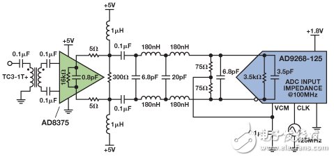
Figure 1. AD8375, AAF, and AD9268 signal chains
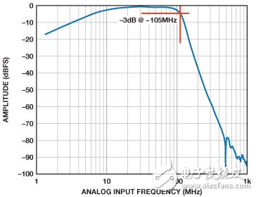
Figure 2. Frequency response of the AD8375, AAF, and AD9268 signal chains
performance
System designers don't expect amplifiers that drive the ADC input to degrade the overall dynamic performance of the system, but the combination of driver and ADC chosen for an application does not mean it can provide the same outstanding performance in another application. Using the techniques described herein, system engineers can estimate expected performance before selecting an amplifier.
Figure 3 shows two different settings. Figure 3(a) uses a passively coupled converter that is the default option for the customer evaluation board. The passive front-end network converts single-ended signals into differential signals using a transformer or balun and a passive low-pass filter with a roll-off frequency of approximately 200 MHz. Figure 3(b) shows the optional amplifier path. The noise contributed by these two settings is compared as follows. The added noise of the amplifier is calculated using a single tone fast Fourier transform (FFT) at low intermediate frequency (10 MHz).
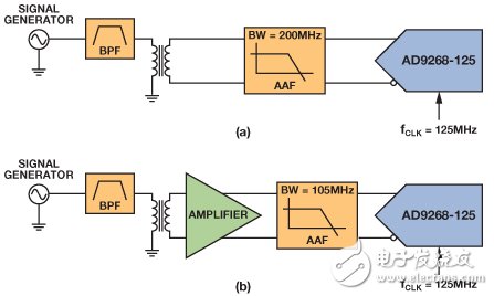
Figure 3. Typical ADC front end: (a) passive; (b) active
Noise analysis typically uses two techniques, but each technique is cumbersome. The noise spectral density (NSD) defines the noise power per unit bandwidth. For ADCs, the unit is the mean square dBm/Hz or dBFS/Hz; for amplifiers, the unit is the root mean square nV/√Hz. This unit of inconsistency constitutes an obstacle to system noise calculation when driving an ADC with an amplifier.
The noise figure (NF) is the logarithmic ratio of the input SNR to the output SNR, expressed in dB. This feature is typically used by RF engineers and makes sense in pure RF environments, but using NF calculations in signal chains with ADCs can lead to misleading results. 2
Another more efficient technique is to "anti-normalize" the noise density and represent it as the rms noise voltage, not the mean square voltage. This method is straightforward and provides a clear analysis of system noise, as explained below.
Figures 4 and 5 show the low frequency tone FFTs of the two front ends, respectively. Note that the passive front end has an SNR of 77.7-dBFS, while the active front end has an SNR of 72.5-dBFS, which is 5.2 dBFS lower than the expected performance of the ADC.
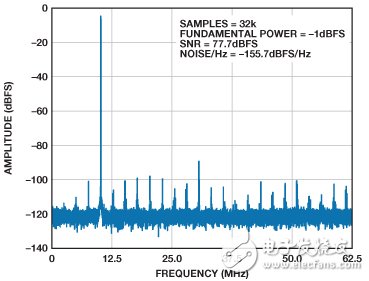
Figure 4. FFT of a 10 MHz analog input tone in Figure 3a
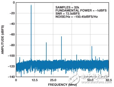
Figure 5. FFT of a 10 MHz analog input tone in Figure 3b
analysisThe only difference between the arrangement shown in Figure 3a and Figure 3b is the addition of an amplifier to the signal chain, so it is safe to say that the performance degradation is caused by the noise of the amplifier. The calculations below help to understand the noise that the amplifier brings.
First, use the converter's full-scale differential input voltage as specified in the data sheet. Dividing the peak-to-peak voltage by 2√2 gives the rms voltage, which is 0.707 V rms.
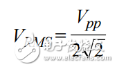 (1)
(1)
Based on the typical SNR of the ADC at 10 MHz, the converter's noise contribution is

(2)
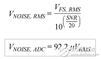
(3)
Using VNOISE, ADC = 92.2 μV rms, system SNR with amplifier front end = 72.5 dBFS, using Equation 3 to calculate system noise yields 168 μV rms.

(4)

(5)
The system noise obtained from Equation 4 is the combined noise of the ADC and VGA. Amplifier noise can be calculated using Equation 5 and results in 140 μV rms. This shows that the amplifier noise is at least 50% larger than the ADC noise, so it is a limiting factor in the system's AC performance.
Note that it is necessary to determine whether the calculated VNOISE, AMP value is consistent with the amplifier's data sheet. The nominal noise spectral density is approximately 20 nV/√Hz at a 150 Ω differential output impedance.
Although the data sheet states that the noise of the VGA does not change substantially with the gain, the noise varies with the load, so the noise spectral density should be scaled according to the total impedance driven by the amplifier output. The amplifier's differential output impedance is large (16 kΩ||0.8 pF), so the impedance seen by the amplifier (see Figure 1) can be calculated as follows:
[10 Ω + (300 Ω | | 150 Ω | | 3.5 kΩ)] = 107 Ω.
Using this value, the derated noise spectral density of the AD8375 in this application can be calculated by Equation 6:

(6)
Note that when calculating the system noise using the actual filter, the shape of the noise bandwidth is different from the ideal filter. This difference in frequency response is defined in the term "shape factor" to reflect noise in the roll-off zone. The shape factor depends on the order of the filter and is the ratio of the noise bandwidth to the –3 dB bandwidth. The more poles of the filter, the closer the shape factor is to 1. This relationship can be seen from Table 1.
Table 1. Relationship between system order and form factor
System order shape factor
1 1.57
2 1.11
31.05
41.03
51.02
The shape factor illustrated in Figure 1 is 1.02. Calculate the noise injected by the amplifier using Equation 6:

This estimated noise value of the VGA injection system is in good agreement with the measured value calculated using Equation 5, demonstrating that the performance of the signal chain consisting of the AD8375 and AD9268 is primarily dependent on the amplifier.
ConclusionIn many cases, the system signal chain requires an amplifier (VGA or gain block) to drive the full-scale signal to the ADC. System designers must understand the degradation of ADC performance caused by different amplifier choices. Before designing with the selected amplifier and ADC, the designer can use the method described herein to calculate the noise distribution of the amplifier and estimate the expected dynamic performance (in SNR) of the intended system implementation.
Zhejiang Best Nail Industrial Co., Ltd. , https://www.beststaple.com
