The 'adaptation' concept design is designed to design a future form of office. Assume that in the near future, a building material will be developed to meet the requirements of thermal insulation and waterproofing, and an intelligent LED technology can be developed to calculate the difference in the day's time through the computer's parameterized calculations. The different illuminances required at the time are then realized on this material in a variety of ways, even endlessly. Specifically, when there is sufficient sunlight, this material will partially block the sunlight according to the settings of the computer program, while the rest will be in a transparent mode; in cloudy days, this material can be Maximizing the area of ​​transparency makes the space behave like a glass box, so that when you work indoors, you are exposed to the natural environment outside.
More importantly, zero consumption is realized in lighting, because the technology that can be directly converted into light energy by absorbing light energy is limited in the LEDs that can be reached today. When lighting at night, part of the energy absorbed by the daytime is insufficient to meet the nighttime. Indoor lighting, therefore, must pass part of the electrical energy to ensure the illumination of the room, so it can not achieve zero consumption from this level; in the sunny day, this material can absorb the energy of sunlight, and then at night, in the In the office, the absorbed energy is converted into light energy to form self-illumination. At this time, one of the possibilities set by the program is selected or manually set, and then applied to the space so that the outdoor is blocked. The illuminance formed by the part of the solar area and the light-transmitting part conforms to the appropriate illuminance of the daytime office. At the same time, the presented spatial form makes the interface form and illumination form of the office space rich and varied. In addition, on clear nights, the program mode is set to full open, local lighting, so that you can enjoy the outdoors at night while working.
In the traditional form of office, reading and writing of text, or sitting in front of a computer all require partial lighting, and then an indirect way to achieve the results of the office. A common example is the desk lamp, which has achieved its function. At the same time, other places were also illuminated. In addition, due to the illumination of local lights, the illumination difference between the illuminated area and the non-illuminated area would be very large, and long-term exposure to this environment would create visual fatigue.
Therefore, can we use the direct method to achieve the office results in the future office work? In the evolution of computers, the solid-state display, keyboard, and mouse are thrown away in return for a two-dimensional operation interface. The self-luminous interface with touch-type controls is presented in the form of three-dimensional display in space. In this way, information can be more intuitively and directly absorbed, which can effectively increase the concentration and work efficiency. In addition, the storage of traditional knowledge in the form of 'e-books' can compress the information of many books in less than 1cm of 'e-books'. The 'e-books' are divided into three parts, up and down. For the light emitting slot and the memory stick, the function of the light emitting channel is to bring the LED light to the display and illuminate the text, pictures and dynamic video; the memory stick is the data for storing the books. Under this technology, the transmission of data becomes Conveniently, no external lighting is required to receive information on books.
'Adapting to' this type of future office can be flexible, fun, fast, intuitive and visually handling various job types.
10 Layer PCB Stack Up thickness, Design and manufacturing
Usually, 10 layer PCB is HDI board, but some are not.
10 Layer PCB Stack Up And Design
Regardless of the number of layers constituting the circuit board design, pad spacing, clearance, trace widths, copper weights and drill hole sizes must be tailored to your contract manufacturer (CM). If your design requires multiple layers, you need to consider additional DFM specifications for signals through vias, power and ground wiring, and PCB stackup.
For 10-layer PCB Manufacturing, it is necessary to determine the number of layers, their arrangement or stacking, and the type of material. These choices require coordination between thickness constraints; material parameters; such as dielectric constant, thermal expansion coefficient and electrical strength; signal type isolation and drilling options. For PCB Assembly , wiring options and their impact on welding process are very important. The function of CM limits the choice of vertical aspect of design.
When your PCB needs six layers of routing, you should choose to use ten layers of PCB. Because ten-layer circuit boards usually have six signal layers and four planes. Of course, we do not recommend the design of more than six signal layers on the 10-layer circuit board. Ten layers are also the largest number of layers, which can be easily manufactured on 0.062 inch thick sheets. Occasionally you will see a 12-layer PCB made of 0.062 inch thick board, but there are not many manufacturers who can make 12-layer circuit boards. Just right, besides making 10-layer circuit boards, we also have very rich experience in manufacturing 12-layer circuit boards.
High layer count boards (10 +) require thin dielectrics (usually 0.006 or smaller on 0.062 thick plates), so they are automatically tightly coupled. After stacking and wiring properly, they can meet all our goals and have excellent EMC performance and signal integrity.
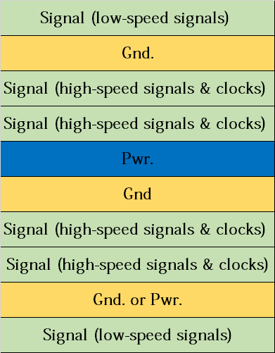
The reason why this stack has such good performance is the tight coupling between signal and return plane, the existence of high-speed shielding signal layer, multiple grounding layers, and tightly coupled power supply/grounding layer pairs in the center of circuit board.
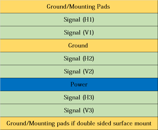
This 10-layer PCB stacking up method abandons closely spaced power/ground pairs. In return, it provides three signal routing layer pairs, shielded by the ground layer on the outer layer of the board, and isolated from each other through the internal power supply and the ground layer.
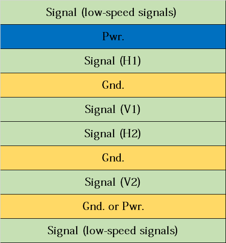
This 10-layer PCB stackup allows the routing of orthogonal signals near the same plane, but in the process, the closely spaced power/ground plane must also be abandoned.
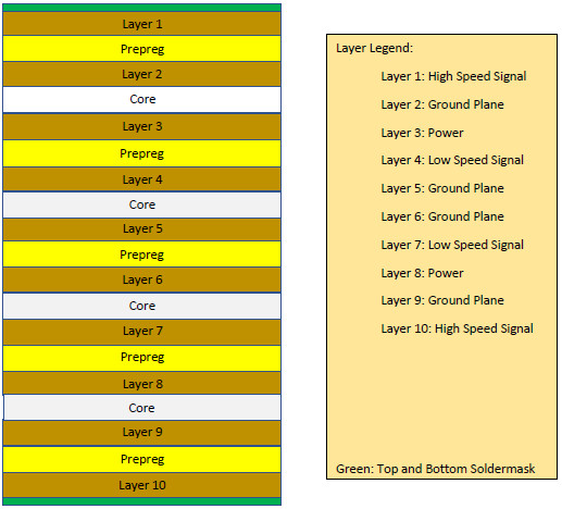
In addition, we list some other stacking methods of 10-layer circuit boards for your reference.
10 Layer PCB Thickness
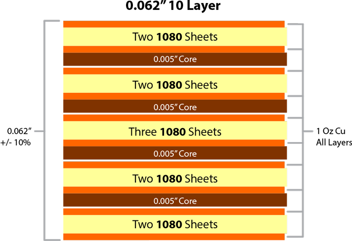
0.062''10 Layer PCB Stackup thickness
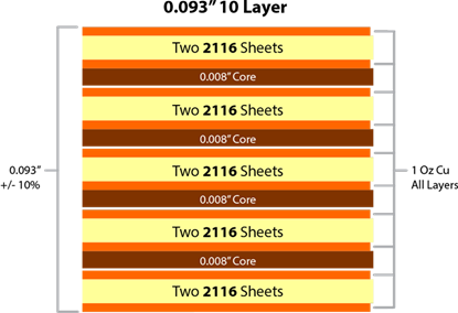
0.093'' 10 Layer PCB Stack UP thickness
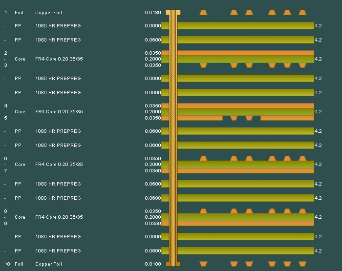
10 Layer Stackup - 1.6mm thickness
layer order
layer name
material type
material description
dielectric constant
thickness
copper weight
1
top
copper
signal
0.035mm
1 oz
7630
prepreg
4.7
0.2mm
2
inner 1
copper
plane
1 oz
core
4.6
0.2mm
3
inner 2
copper
plane
1 oz
2116
prepreg
4.5
0.12mm
4
inner 3
copper
plane
1 oz
core
4.6
0.2mm
5
inner 4
copper
plane
1 oz
2116
prepreg
4.5
0.12mm
6
inner 5
copper
plane
1 oz
core
4.6
0.2mm
7
inner 6
copper
plane
1 oz
2116
prepreg
4.5
0.12mm
8
inner 7
copper
plane
1 oz
2116
prepreg
4.6
0.2mm
9
inner 8
copper
plane
1 oz
7630
prepreg
4.7
0.2mm
10
bottom
copper
signal
0.035mm
1 oz
Final board thickness: 1.6mm±0.16mm
10 Layer PCB Application
With the rapid development of today's increasingly complex multi-layer PCB, machines and equipment in various industries - commerce, industry, medicine, government, Aerospace - continue to grow in terms of speed, capacity, compactness and ease of use.
8, 10 and 12 layers of multi-layer PCB are useful in many high-tech equipment and computer systems. In recent decades, the development of multi-layer Printed Circuit Boards has led to the rapid development of computer technology - from the previous Gigabit system to today's GHz machine.
Especially 10-layer PCB, which is widely used in the following industries: Preamplifier, Satellite Dish, GPS Tracking Devices, SAN Storage, AC Drives, GSM Signal Booster, Mobile Broadband Router, Inverter 220V, Memory Module, Automotive dashboards
Cheap 10 Layer PCB manufacturing services
For customized printed circuit boards, our 10-layer PCB offers the fastest turning time for the best price we can offer. For on-demand pricing and ordering of your next Printed Circuit Board project, you can contact our online customer support or send us an email to get 10-layer PCB quotation immediately.
10 Layer PCB
Printed Wire Board,Custom PCB Board,10 Layer PCB,10 Layer PCB Stackup
JingHongYi PCB (HK) Co., Limited , https://www.pcbjhy.com

