Skilled Tips Tips
Study packaging process to increase allowable loss
The heat loss of the linear regulator depends on the input voltage, output voltage, and output current.
Heat loss (Pd) = (input voltage - output voltage) × output current
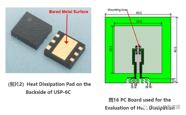
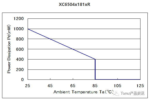
In fact, how to improve the heat dissipation of the package when manufacturing the instrument is extremely important. USP packages are included in the package that efficiently dissipates heat. The metal chip on which the IC wafer is mounted on the back of the package is exposed to the outside and can dissipate heat from the chip to the PCB substrate. (Photo 2) The heat dissipation is determined by the metal area of ​​the PCB substrate. Figure 15 shows the heat dissipation characteristics of the USP-6C package. For the USP-6C itself, there is an allowable loss of 120mW. When the area of ​​the thin copper sheet is 800mm2, the loss is 1W. Increasing the area of ​​the thin copper sheet can obtain a greater allowable loss. The circuit board used as the evaluation loss is described in FIG.


Figure 15 Heat Dissipation Characteristics: USP-6C Package
Laser trimming
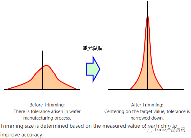
The output voltage of the CMOS linear regulator has been pre-set. The output voltage cannot be adjusted with an external resistor, but is compensated by the 0.1V or 0.05V output voltage interval. This is due to the application of laser trimming technology that makes it easy to set arbitrary high-precision voltages. Because it is difficult to make a stable reference voltage similar to that of the bipolar transistor bandgap reference voltage shown in (Note 1) in the CMOS process, changing the resistance for presetting the output voltage to laser trimming can disperse the internal reference voltage irregularly The value is set to an arbitrary voltage value, and it is also a general method of ensuring the accuracy of the output voltage. (Figure 17)
The output voltage accuracy of general products is ±2%, and that of high-precision products is ±1%. Depending on the product, the output voltage accuracy is specified for different operating temperature ranges.
(Note 1) Bandgap reference voltage
By using the power band gap and the resistance of the bipolar transistor, the voltage temperature coefficient, which is proportional to the absolute temperature, is used to obtain a stable voltage circuit corresponding to the temperature.

Figure 17 The Image of Tolerance Compensation by Lazar Trimming Technology
Which voltage regulators are easy to purchase when purchased in small quantities?
Because almost all output voltages cannot be adjusted externally, inventory status must be confirmed at the time of purchase. The commonly available output voltage is 5V, 3.3V, 3V, 2.8V, 2.5V, 1.8V, 1.2V.
Future developments
The miniaturization of CMOS process LSIs is progressing every year, and mass production of products called 22nm specifications has begun. For power supply ICs such as linear regulators, the input power supply must withstand voltage. Although extremely fine processes are not necessarily considered to be all beneficial, using CMOS's microtechnology advantages, processes such as 0.25μm or 0.35μm can be achieved. With a 1.7V input voltage, an output voltage of 1.2V and a current of 2A can be provided. In addition, in terms of high withstand voltage, various new technologies and advantages of using CMOS's advanced technology have also been introduced.
The CMOS process is used in the development of LSI or memory, and has accumulated a large number of process technologies. It can be predicted that CMOS regulators will be used in a wider area than mobile devices.
Industrial Diesel Generator,Industrial Generators,Commercial Diesel Generators,Industrial Type Diesel Generator
Jiangsu Vantek Power Machinery Co., Ltd , https://www.vantekpower.com
