Here are some typical processing procedures of digital TV.
Figure 07-04-9 is a block diagram of digital processing in the studio. The signal source sends R, G, and B signals to the color camera, which are converted into digital video signals by A / D and sent to the program production unit. At the same time, the signals from the digital video recorder, digital special effects, and digital system converters are all sent in. In the program production unit, the signal after the production of the program is sent to the D / A converter to become an analog signal, and then sent to the TV transmitter.
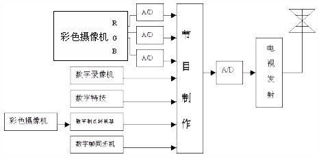
Figure 07-04-9 Studio digital processing block diagram
Figure 07-04-10 is a block diagram of a digital TV transmission system. The originator produces color TV images from the camera. After A / D conversion, it becomes a digital video signal and is sent to the source code. The source code undertakes the compression function of the image data, it removes the redundant part in the signal, and reduces the transmission code rate. The image signal encoded by the source is sent to the multiplexer for multiplexing with the digital audio signal, and then sent to the channel encoder. The channel coding is error correction coding, which improves the anti-interference ability of the signal during transmission. . This is because the data code stream inevitably introduces noise after long-distance transmission and bit errors occur. Therefore, an error correction code is added to improve its anti-interference ability. The signal after error correction coding is sent to the output interface circuit. The output interface circuit plays a role of code type conversion, that is, the unipolar code is changed into a bipolar code which is favorable for transmission. For long-distance transmission, digital microwave lines or digital optical fiber lines can be used, and the distance between stations can reach 50 kilometers by relay transmission. The process of the receiving end is opposite to the sending end. After the receiving end receives the signal, the input interface circuit converts the bipolar signal into a unipolar signal, and then sends it to the channel decoding. In the channel decoding, the error code caused by transmission can be corrected, The signal is sent to demultiplexing, and then sent to the video and audio processing circuits, respectively, and restored to analog video and audio signals.
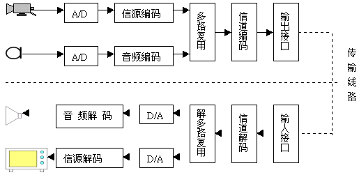
Figure 07-04-10 Block diagram of digital TV transmission system
The block diagram of the digital TV receiver is shown in Figure 07-04-11. The signal received by the TV receiving antenna is amplified by the high frequency channel and the intermediate frequency, and then sent to the video detection to obtain the analog signal. After A / D conversion, it becomes a digital signal, which is sent to a digital processor for digital noise reduction, digital contour correction, digital de-ghosting, line frequency doubling, de-flicker processing, picture-in-picture processing, etc. In the D / A converter, it becomes an analog signal for display by the picture tube. The high-frequency part of the TV transmitter and the high-frequency channel part of the TV receiver are both analog systems. This is because it is impossible to achieve digitalization at a frequency close to 1000 MHz at the current technical level.
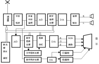
Figure 07-04-11 Block diagram of digital TV receiver
Encoding digital TV signals can be divided into full signal encoding and component encoding, as shown in Figure 07-04-12. Figure (a) is full signal coding, and Figure (b) is component signal coding. It can be seen from the figure (a) that the analog full TV signal is converted into a digital signal by A / D conversion, and after digital processing, it is sent to the D / A conversion to restore the analog full signal. The full signal encoding seems simple from the block diagram, but this method is easy to cause bright and color interference. Especially for the SECAM system (color TV system in Eastern European countries), since the modulation method of the sub-carrier frequency by the color-difference signal is frequency modulation, it is difficult to use full-signal encoding and only component encoding. Figure (b) is a block diagram of component signal encoding. After the analog full signal is A / D converted, it is then digitally bright and color separated, divided into a digital brightness signal and a digital color difference signal, and sent to a digital signal processor. The processed signal Then it is coded by digital full signal, and then it becomes analog full signal by D / A. Although the figure adds digital bright, color separation and digital full-signal encoding, digital processing is performed on the component signals, eliminating the phenomenon of bright and color interference. This processing method can improve the image quality, so it is widely used, and international standards also recommend the use of component signal encoding.
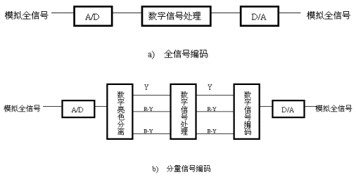
Figure 07-04-12 Full signal encoding and component encoding
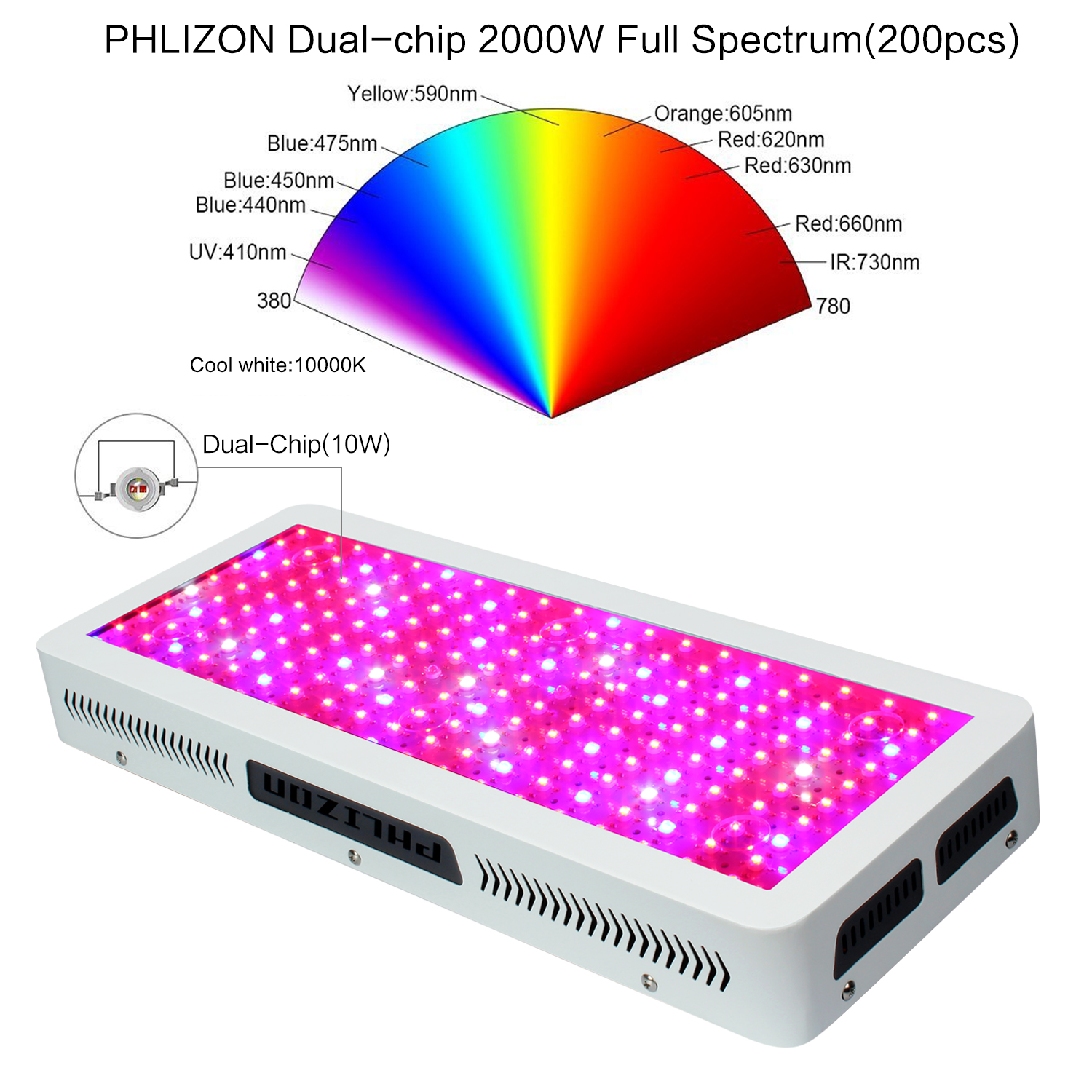
Cree Led Grow Light can save about 30% cost in the application,mainly lie in LED package cost,light engine production costs and the secondary light distributioncosts, which is great significance for applications and promotion of semiconductor lighting. We could also DIY the led ratio(wavelength ratio) which imitate the natural sun spectrum to help your plants grow in a very natural type of atmosphere, Absolutely, we are the very original and professional OEM/ODM factory, our Cree Led Grow Light have the great cost performance with the new integration technology being used for mass production, partners around the world keep telling us how amazed at the increase in output and the decrease in the energy bill.
Applications
Our professional full spectrum CREE LED Grow Light are suitable for all the indoor plants and good for seeding, growth,flowering and fruiting stages of plants, increasing the harvest and Saving energy.
Key Features
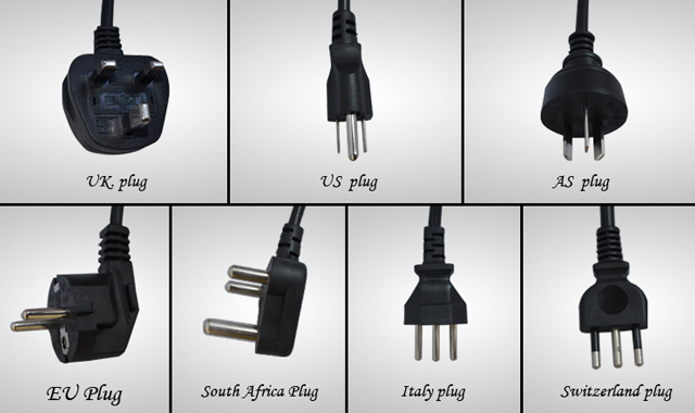
Plug with listed certificate safe to use.
Item Display
The Plug you can choose
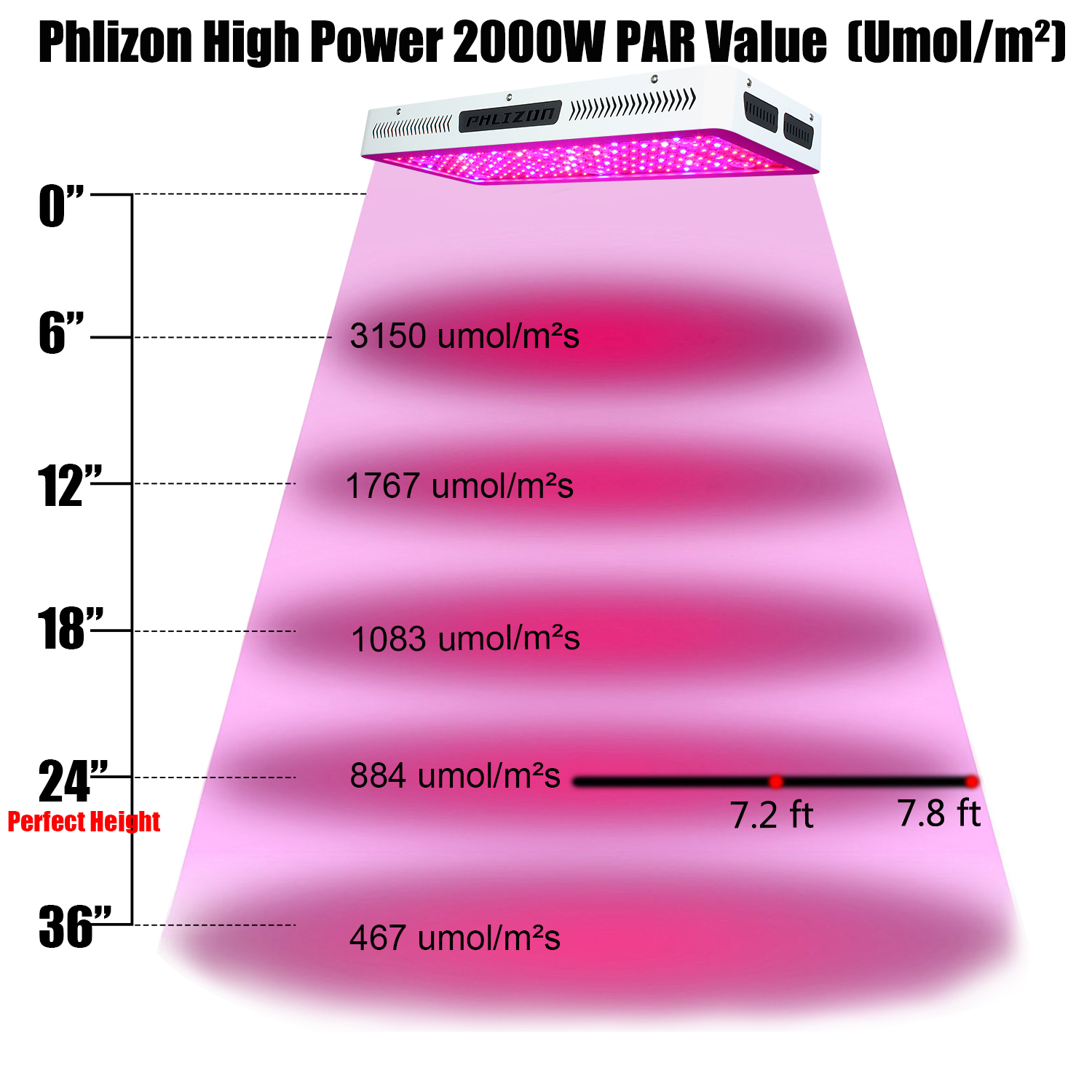
Full Spectrum Cree LED Grow Light PAR Value
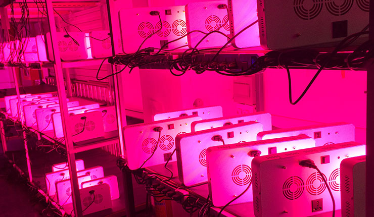
Our Ageing Test
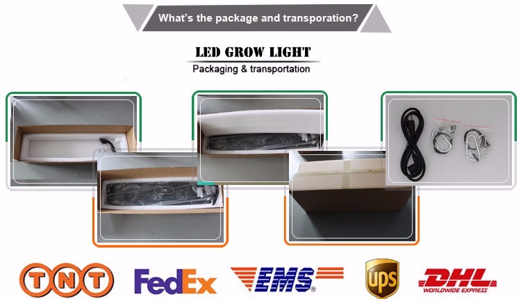
Package
Warnings:
1.lndoor use only.
2.To avoid being damaged,do not use water or drip irrigation while using.
3.Sunshine lighting time should be 12-18 hours.
4.While irradiating the plants,the height of led grow lamp is not less than 10 inches,low height will cause the destruction of plants.
5.Highly hang the lamp will weaken the energy and affect the growth cycle of the plants, so the lamp should not be hung too high.
6.While taking care of the plants, please spray the leaves and branches 2-3 times everyday,to ensure the the plants do not wrinkle a wither, and have no phenomenon of few fruit, and hard pericarp.
Warmly welcome to Visit our Factrory when you come to China.
Cree Led Grow Light
CREE Chips LED Grow Light,CREE LED Grow Light,CREE Grow Light,CREE COB LED Grow Light
Shenzhen Phlizon Technology Co.,Ltd. , https://www.philizon.com
