This article continues to talk about the implementation details of the physical layer logic sublayer of the receiving end. Recall the previous picture:
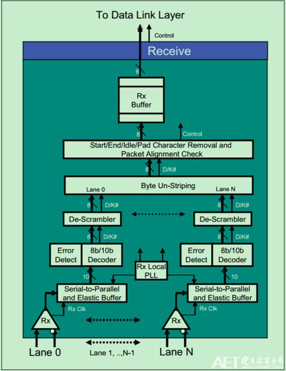
The specific logic of one of the Lanes is shown in the figure below:
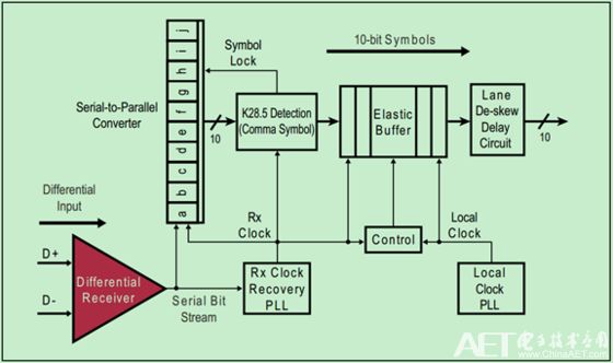
Among them, Rx Clock Recovery extracts Rx Clock from the input serial data stream. When Rx Clock is stable on the frequency of Tx Clock (Rx Clock locked on to the Tx Clock Freq), we say that the receiver has obtained Bit Lock.
If the link is in a low-power state (such as L0s or L1), the receiver will lose synchronization (Losing Bit Lock) at this time. In order to prevent the physical layer from thinking that this is an error (abnormality), the sender sends an Electrical Idle Ordered Sets (EIOS) to notify the receiver that it is about to enter a low-power state. At this point, the receiver temporarily de-gates its input.
Note: De-gate here does not directly close the input port, but temporarily does not process the data on the input port.
When the sender needs to wake up the link, a certain number of FTS Ordered Sets will be sent first, and Bit Lock and Symbol Lock will be re-acquired.
The receiver's link De-Skew logic is shown in the figure below:
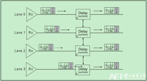
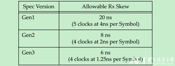
The Gen1 and Gen2 PCIe use COM characters for De-Skew. If COM does not appear on each Lane, the first arriving COM will be delayed for a while to achieve Lane synchronization. Obviously, this mechanism can only correct relatively small Skew, that is to say, the Skew of Lane-to-Lane has a maximum value. Beyond this maximum value, De-Skew cannot do anything. The following table shows:
Receiver 8b/10b decoder structure as shown below:
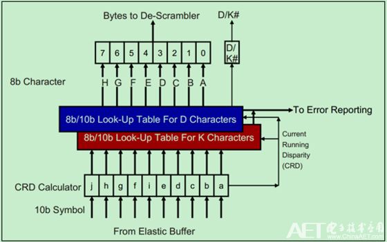
The following conditions are considered as Code Violation, which means that the character has encountered an error during transmission:

The descramblers and Byte Un-striping are relatively simple and are not described in detail here. Specifically refer to the relevant content of PCIe Spec.
Shenzhen Kate Technology Co., Ltd. , https://www.katevape.com
