Abstract: This applicaTIon note describes how ESD threatens electronic systems, type of damage inflicted, how ESD is generated, test methods and waveforms used, human body and machine models for tesTIng, IEC compliance levels, contact and air discharge. ProtecTIon methods are described and Maxim's approach to ESD protecTIon is detailed. Guidelines are given for selecting ICs with high resistance to ESD. RS-485 ports and analog switches and multiplexers are specifically considered.
Electrostatic discharge (ESD) is often found to be the root cause of equipment failure on the factory floor and in the field. Such failures can be difficult to track down when they masquerade as other types of failures, as they often do. In manufacturing, for instance, the yield loss at final test might be traced to a bad component or subassembly and then (with further investigation) associated with an OEM manufacturing or test process that subjects the part to ESD.
Early field failures and post-installation problems in industrial equipment are often caused by ESD during installation. The most insidious ESD damage is that which degrades the performance of an instrument but (at least initially) does not affect its operation in an obvious way. Such events can cause erratic or nonlinear operation immediately but may not produce a "hard" failure for months or years.
This article explains how to protect your products from ESD. It outlines the standard test methods required by the electronics industry, offers some common techniques to protect against ESD, and highlights some of Maxim's patented ESD-protected devices. With careful design, these devices can improve product quality while saving money and your company's reputation.
Damage Potential A photomicrograph (Figure 1) shows the damage sustained by a competitor's RS-232 interface IC after exposure to an ESD strike of 15kV (a common test level). The result is a gross failure that is easily visible, because the overstress actually vaporized metalization on the chip. In other cases, the investigation of invisible failures in the gate-oxide layers or buried layers requires careful removal of metalization or other layers. ESD strikes can also find paths into the core of an instrument. Somewhat like a lightning strike, ESD will course through the circuit until its energy is dissipated, often with unexpected effects.
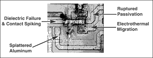
Figure 1. This photomicrograph shows gross ESD damage to an unprotected RS-232 receiver.
Where Does High Voltage Come From? Mechanically separating two materials creates electrostatic charge. The surfaces of these otherwise neutral materials are electrically double-layered to varying degrees, meaning that the outer layer might have a majority of electrons balanced by positive charge in the bulk of the material. Other materials exhibit the opposite surface charge. When materials with opposite surface charges come in contact, a transfer of electrons leaves one material with a net negative charge and the other with a net positive charge. Called triboelectric generation, this effect is the basis of static generation and transfer.
The triboelectric series shown in Table 1 positions materials like glass and nylon at the positive end and silicon and teflon at the negative end. The materials' conductivity also affects their ability to build up a surface charge. For many materials, the conductivity or surface resisitivity is strongly dependent on humidity. Low humidity promotes low conductivity, which maintains the localized charges by preventing them from moving.
Table 1. Triboelectric Series
In the real world, static high voltage is produced usually by the interaction of people and their surroundings. Imagine a person sitting at a formica table in a plastic chair, wearing wool slacks and socks, leather shoes, a cotton shirt, and a silk tie . This soup of triboelectric materials defies quantitative analysis, but one can imagine it responsible for some serious charge buildup. Several accepted models describe a charged human body for different situations. The most generic model (Figure 2) assumes a 100pF capacitance charged to 15,000V and a 1500Ω series resistance.
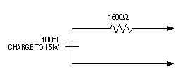
Figure 2. When discharged, this circuit (the Human Body Model) produces a very fast rise time with current peaks of 15kV / 1.5kΩ—over 10A!
Test Methods and Standards Two methods used commonly for testing the ESD susceptibility of integrated circuits have been adapted for end-equipment testing, as outlined in the next section. The oldest method, MIL-STD-883 Method 3015.7, was developed as an aid in understanding the precautions necessary for packaging and handling ICs. This method tests each package pin against other groups of pins and classifies the device according to the lowest voltage for which failure occurs.
The applied signal in this test is a current waveform derived from a circuit called the Human Body Model (Figure 2), which simulates the capacitance and the source impedance typical of a human body. Circuit layout is critical, because the actual waveform delivered at the IC also depends on parasitic inductance and capacitance associated with the test connections and PC board. The resulting current waveform represents the ESD that occurs when a person touches an object such as an IC.
The other method, which differs from the above only in the values ​​for R and C, was developed by the Electronic Industries Association of Japan (EIAJ). Called IC-121 and based on a circuit called the Machine Model (Figure 3), it applies a current waveform similar to that produced when an IC makes contact with its handling machinery. By mimicking the ESD events caused by charges that accumulate on moving parts, the waveform simulates the static discharges seen during machine assembly.
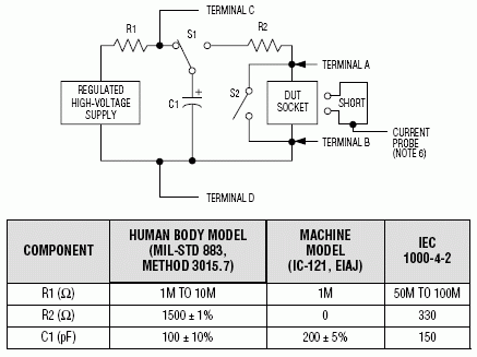
Figure 3. Substituting different component values ​​as shown yields discharge circuits known as the Human Body Model, the Machine Model, and the IEC 1000-4-2 Model (human holding a metallic object).
The two methods are complementary, so you shouldn't choose one over the other. Because ESD can affect ICs during manufacturing, during PC board assembly, and after the end product is put into service, a test based on the Human Body Model and the Machine Model together provides adequate assurance regarding the IC's tolerance for the rigors of manufacturing and product life.
These two tests are for ICs. Other specific tests govern the exposed interfaces of end equipment. For example, IC pins exposed to the outside world through connectors can encounter ESD even when mounted on a PC board within an enclosure. ESD exposure is less likely for the other pins, which are connected to circuitry on the board.
For this class of IC, a test method such as Method 3015.7 (which tests pin combinations) does not provide an adequate representation of ESD susceptibility for the input / output (I / O) pins. The Machine Model and Method 3015.7, which offer ratings according to the lowest voltage failure on any pin, may not do justice to the higher levels of internal ESD protection required by the I / O pins (and provided by some manufacturers). A device might have I / O pins that withstand ± 15kV and non-I / O pins that fail at ± 2kV. With the methods described above, the resulting ESD rating could be less than ± 2kV. Fortunately, however, better test methods are now available for rating I / O pins.
New ESD Tests for I / O PortsAn I / O port allows communication with other pieces of equipment. I / O ports for ICs Includes logical groups of pins that give access to equipment external to the system containing the IC. These pins are subject to static discharge and other abuse, as operators connect and disconnect cables from the system. For the I / O pins of an external interface IC, an ideal test method for ESD susceptibility would accomplish the following:
Test the I / O pins only in ways that simulate exposure to ESD events in actual equipment. Apply test waveforms that model electrostatic discharges produced by the human body. Different circuit models specify different values ​​of amplitude, rise / fall time, and transferred power. Test the IC with and without power applied. Define IC failures to include latchup (a momentary loss of operation) as well as catastrophic or parametric failure. Latchup is considered a failure mechanism, because, if left undetected, it can lead to reliability problems and system malfunctions. Two methods—both compliant with the requirements listed—have seen increasing use by equipment manufacturers in testing the ESD susceptibility of I / O ports (Figure 3). The first is a modification of Method 3015.7, MIL-STD-883. It makes use of the same circuit model and waveform as the original method but applies ESD pulses only to the I / O pins of a device. Its intent is to simulate the fault currents seen by an IC installe d on a board and operating in the target system. The second method is IEC 1000-4-2, which has become the world standard. It specifies a higher capacitance and a lower resistance than that specified in Method 3015.7. IEC 1000-4- 2 is applied universally in testing end-equipment interfaces (Table 2). Note that Maxim's analog switches and RS-232 / RS-485 interface ICs comply with these ESD standards, without the need for external components.
Table 2. IEC 1000-4-2 Classification of Four Voltage Ranges
ESD-Protection Methods Protecting an interface from ESD damage is the designer's responsibility. The industry offers a choice of several methods, each with certain strengths and weaknesses. Lots of misunderstanding and black magic surround ESD remedies; the following discussion is intended to dispel some of that mystery.
Capacitor Protection
This method is common in high-volume consumer and automotive equipment. It protects the input pins with a simple shunt capacitor from input to ground. The idea is that a capacitor of sufficient value will absorb an ESD discharge without exceeding the ESD rating of the attached IC pin. To illustrate, consider an IC pin exposed to the outside world, with an ESD rating of 2kV.
The IEC 1000-4-2 Model specifies a 150pF capacitance charged to 15kV. If a 1500pF capacitance is added to the exposed pin, it will charge to a maximum equal to 1/10 of the test voltage (1.5kV). Because this level is below the IC's ESD-protection rating, one assumes that all is well. This method is used widely, but it involves a simplistic view of the physics involved. It gives some protection if you exercise extreme care in the circuit layout, provided that the circuit operation is not affected by either the necessary capacitance or parasitic inductance. To emphasize the sensitivity to layout, consider that a 1cm trace on a PC board has about 7nH of inductance. When a 30A current pulse with 1ns rise time (the IEC 1000- 4-2 waveform, Figure 4) is applied to 7nH, it produces a voltage spike of 210V for each centimeter of ground path.
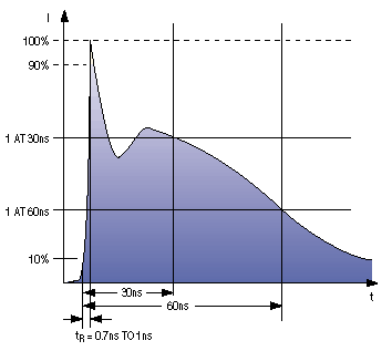
Figure 4. Parameters for this ESD waveform (rise time, peak current, amplitude at 30ns, and amplitude at 60ns) are specified by IEC 1000-4-2.
Resistor Protection
Resistor protection is added in series to the interface pins. This resistance limits peak currents and helps dissipate some of the power in a transient. As with capacitor protection, precautions should be taken to ensure that circuit operation is not affected adversely by this increased impedance. Another caveat is that resistors themselves can be ESD-sensitive. Metal-film resistors are fabricated with methods similar to semiconductor metalization and often have similar ESD limitations. The parasitic capacitance of these series resistors can also be an issue. A narrow spike, through even a few picofarads, can wreak havoc on an IC input.
Resistor-Capacitor Protection
This approach is a hybrid of the R and C protection techniques discussed above. Having two components per interface pin consumes PC real estate while increasing costs and decreasing reliability. RC networks are often used for EMI suppression in concert with ferrite beads or feedthroughs.
MOVs and TransZorb â„¢ Protection
Adding metal-oxide varistors (MOVs) or silicon avalanche suppressors (TransZorbs) to I / O pins can be very effective. They tend to be expensive, can be large, and can add unwanted capacitance to an interface. As with capacitor protection, these devices require low-inductance (short) paths to ground.
Layout Guidelines for Enhancing ESD Protection
Follow standard analog-layout techniques, placing all bypass and charge-pump capacitors as close as possible to the IC (interface ICs especially). Include a ground plane on the PC board. Place the protection or IC as close to the I / O port as possible. Protection Internal to Maxim ICsMaxim has invested a substantial effort in developing ICs with internal ESD protection. Starting with RS-232 and RS-485 interface ICs, these protected devices now include several analog switches and the MAX681_ family of switch debouncers. All withstand the application of IEC 1000-4-2 ESD events directly to their I / O pins. Maxim believes this is the best way to control ESD in a system. It is robust, readily available, requires no external real estate, and costs less than most alternatives.
Maxim offers a variety of ESD-protected RS-232 interface ICs, representing every useful combination of drivers and receivers. Included are ultra-low-power RS-232 devices incorporating Maxim's AutoShutdown â„¢ feature. Several new innovations have been introduced in the area of ESD-protected RS-232 interface devices this year. For example, single RS-232 receivers and transmitters with full ESD protection in tiny SOT packages (the MAX318_ series) can be real problem solvers in small portable equipment.
Also scheduled for introduction is a unique ESD-protected interface for data cables. Data cables for cellular phones usually include an RS-232 interface in the cable rather than the phone. Thus, ESD protection for this application is required not just on the RS- 232 side of the interface IC but on the logic side as well. The MAX3237E is the only IC available that provides a solution to this problem. It offers a complete five-transmitter, three-receiver interface (like a modem). Maxim has plans to introduce additional RS-232 interface ICs with this double ESD protection for other applications such as PDA cradles and other phone configurations.
RS-485 Interfaces Maxim is also the leader in ESD-protected RS-485 interfaces. After pioneering the use of ESD protection for such devices, Maxim offers 17 products in this area, with many more on the way. Significant over the last year was the introduction of the MAX3095 / MAX3096, which extend Maxim's robust ESD structures and low-power operation to the venerable 26LS32 quad-receiver pinout. Also released last year was a full line of 3.3V, ESD-protected, RS-485 interface ICs. Maxim innovations for the MAX348_E family, for example, include ESD protection, fractional unit loads, slew-rate limiting, and low power.
Analog Switches Maxim was the first IC company to recognize the value of ESD protection for analog switches and multiplexers that serve as the interface to external systems in a host of applications for which ESD protection is necessary. First was a series of ESD-protected switches and multiplexers. This series includes several low-voltage ICs with ± 15kV ESD protection: an 8-to-1 CMOS analog multiplexer with 4051 pinout (MAX4558), a 4-to-1 CMOS analog multiplexer with 4052 pinout (MAX4559), a triple SPDT switch with 4053 pinout (MAX4560), and an SPST, CMOS analog switch with 4066 pinout (MAX4551).
A second series of devices, in SOT23 packages with ± 15kV ESD protection, includes a single SPST-NO switch (MAX4568), an SPST-NC switch (MAX4569), and an SPDT switch (MAX4561).
References Maxim Engineering Journal # 25, "ESD Protection for I / O Ports."
Electrostatic Discharge Control, Owen J. McAteer, McGraw Hill. 1989. ISBN 0-07-044838-8.
Electrostatic discharge (ESD) is often found to be the root cause of equipment failure on the factory floor and in the field. Such failures can be difficult to track down when they masquerade as other types of failures, as they often do. In manufacturing, for instance, the yield loss at final test might be traced to a bad component or subassembly and then (with further investigation) associated with an OEM manufacturing or test process that subjects the part to ESD.
Early field failures and post-installation problems in industrial equipment are often caused by ESD during installation. The most insidious ESD damage is that which degrades the performance of an instrument but (at least initially) does not affect its operation in an obvious way. Such events can cause erratic or nonlinear operation immediately but may not produce a "hard" failure for months or years.
This article explains how to protect your products from ESD. It outlines the standard test methods required by the electronics industry, offers some common techniques to protect against ESD, and highlights some of Maxim's patented ESD-protected devices. With careful design, these devices can improve product quality while saving money and your company's reputation.
Damage Potential A photomicrograph (Figure 1) shows the damage sustained by a competitor's RS-232 interface IC after exposure to an ESD strike of 15kV (a common test level). The result is a gross failure that is easily visible, because the overstress actually vaporized metalization on the chip. In other cases, the investigation of invisible failures in the gate-oxide layers or buried layers requires careful removal of metalization or other layers. ESD strikes can also find paths into the core of an instrument. Somewhat like a lightning strike, ESD will course through the circuit until its energy is dissipated, often with unexpected effects.

Figure 1. This photomicrograph shows gross ESD damage to an unprotected RS-232 receiver.
Where Does High Voltage Come From? Mechanically separating two materials creates electrostatic charge. The surfaces of these otherwise neutral materials are electrically double-layered to varying degrees, meaning that the outer layer might have a majority of electrons balanced by positive charge in the bulk of the material. Other materials exhibit the opposite surface charge. When materials with opposite surface charges come in contact, a transfer of electrons leaves one material with a net negative charge and the other with a net positive charge. Called triboelectric generation, this effect is the basis of static generation and transfer.
The triboelectric series shown in Table 1 positions materials like glass and nylon at the positive end and silicon and teflon at the negative end. The materials' conductivity also affects their ability to build up a surface charge. For many materials, the conductivity or surface resisitivity is strongly dependent on humidity. Low humidity promotes low conductivity, which maintains the localized charges by preventing them from moving.
Table 1. Triboelectric Series
Air (most pos.) | Fur | Sealing wax | Orlon |
Hands | Lead | Hard rubber | Saran |
Asbestos | Silk | Nickel, copper | Polyurethane |
Rabbit fur | Aluminum | Brass, silver | Polyethylene |
Glass | Paper | Gold, platinum | PVC |
Mica | Cotton | Sulfur | KEL-F (CTE) |
Human hair | Steel | Acetate, rayon | Silicon |
Nylon | Wood | Polyester | Teflon (most neg.) |
Wool | Amber | Celluloid |
In the real world, static high voltage is produced usually by the interaction of people and their surroundings. Imagine a person sitting at a formica table in a plastic chair, wearing wool slacks and socks, leather shoes, a cotton shirt, and a silk tie . This soup of triboelectric materials defies quantitative analysis, but one can imagine it responsible for some serious charge buildup. Several accepted models describe a charged human body for different situations. The most generic model (Figure 2) assumes a 100pF capacitance charged to 15,000V and a 1500Ω series resistance.

Figure 2. When discharged, this circuit (the Human Body Model) produces a very fast rise time with current peaks of 15kV / 1.5kΩ—over 10A!
Test Methods and Standards Two methods used commonly for testing the ESD susceptibility of integrated circuits have been adapted for end-equipment testing, as outlined in the next section. The oldest method, MIL-STD-883 Method 3015.7, was developed as an aid in understanding the precautions necessary for packaging and handling ICs. This method tests each package pin against other groups of pins and classifies the device according to the lowest voltage for which failure occurs.
The applied signal in this test is a current waveform derived from a circuit called the Human Body Model (Figure 2), which simulates the capacitance and the source impedance typical of a human body. Circuit layout is critical, because the actual waveform delivered at the IC also depends on parasitic inductance and capacitance associated with the test connections and PC board. The resulting current waveform represents the ESD that occurs when a person touches an object such as an IC.
The other method, which differs from the above only in the values ​​for R and C, was developed by the Electronic Industries Association of Japan (EIAJ). Called IC-121 and based on a circuit called the Machine Model (Figure 3), it applies a current waveform similar to that produced when an IC makes contact with its handling machinery. By mimicking the ESD events caused by charges that accumulate on moving parts, the waveform simulates the static discharges seen during machine assembly.

Figure 3. Substituting different component values ​​as shown yields discharge circuits known as the Human Body Model, the Machine Model, and the IEC 1000-4-2 Model (human holding a metallic object).
The two methods are complementary, so you shouldn't choose one over the other. Because ESD can affect ICs during manufacturing, during PC board assembly, and after the end product is put into service, a test based on the Human Body Model and the Machine Model together provides adequate assurance regarding the IC's tolerance for the rigors of manufacturing and product life.
These two tests are for ICs. Other specific tests govern the exposed interfaces of end equipment. For example, IC pins exposed to the outside world through connectors can encounter ESD even when mounted on a PC board within an enclosure. ESD exposure is less likely for the other pins, which are connected to circuitry on the board.
For this class of IC, a test method such as Method 3015.7 (which tests pin combinations) does not provide an adequate representation of ESD susceptibility for the input / output (I / O) pins. The Machine Model and Method 3015.7, which offer ratings according to the lowest voltage failure on any pin, may not do justice to the higher levels of internal ESD protection required by the I / O pins (and provided by some manufacturers). A device might have I / O pins that withstand ± 15kV and non-I / O pins that fail at ± 2kV. With the methods described above, the resulting ESD rating could be less than ± 2kV. Fortunately, however, better test methods are now available for rating I / O pins.
New ESD Tests for I / O PortsAn I / O port allows communication with other pieces of equipment. I / O ports for ICs Includes logical groups of pins that give access to equipment external to the system containing the IC. These pins are subject to static discharge and other abuse, as operators connect and disconnect cables from the system. For the I / O pins of an external interface IC, an ideal test method for ESD susceptibility would accomplish the following:
Test the I / O pins only in ways that simulate exposure to ESD events in actual equipment. Apply test waveforms that model electrostatic discharges produced by the human body. Different circuit models specify different values ​​of amplitude, rise / fall time, and transferred power. Test the IC with and without power applied. Define IC failures to include latchup (a momentary loss of operation) as well as catastrophic or parametric failure. Latchup is considered a failure mechanism, because, if left undetected, it can lead to reliability problems and system malfunctions. Two methods—both compliant with the requirements listed—have seen increasing use by equipment manufacturers in testing the ESD susceptibility of I / O ports (Figure 3). The first is a modification of Method 3015.7, MIL-STD-883. It makes use of the same circuit model and waveform as the original method but applies ESD pulses only to the I / O pins of a device. Its intent is to simulate the fault currents seen by an IC installe d on a board and operating in the target system. The second method is IEC 1000-4-2, which has become the world standard. It specifies a higher capacitance and a lower resistance than that specified in Method 3015.7. IEC 1000-4- 2 is applied universally in testing end-equipment interfaces (Table 2). Note that Maxim's analog switches and RS-232 / RS-485 interface ICs comply with these ESD standards, without the need for external components.
Table 2. IEC 1000-4-2 Classification of Four Voltage Ranges
IEC 1000-4-2 Compliance Level | Max Test Voltage, Contact Discharge (kV) | Max Test Voltage, Air GAP Discharge (kV) |
1 | 2 | 2 |
2 | 4 | 4 |
3 | 6 | 8 |
4 | 8 | 15 |
Capacitor Protection
This method is common in high-volume consumer and automotive equipment. It protects the input pins with a simple shunt capacitor from input to ground. The idea is that a capacitor of sufficient value will absorb an ESD discharge without exceeding the ESD rating of the attached IC pin. To illustrate, consider an IC pin exposed to the outside world, with an ESD rating of 2kV.
The IEC 1000-4-2 Model specifies a 150pF capacitance charged to 15kV. If a 1500pF capacitance is added to the exposed pin, it will charge to a maximum equal to 1/10 of the test voltage (1.5kV). Because this level is below the IC's ESD-protection rating, one assumes that all is well. This method is used widely, but it involves a simplistic view of the physics involved. It gives some protection if you exercise extreme care in the circuit layout, provided that the circuit operation is not affected by either the necessary capacitance or parasitic inductance. To emphasize the sensitivity to layout, consider that a 1cm trace on a PC board has about 7nH of inductance. When a 30A current pulse with 1ns rise time (the IEC 1000- 4-2 waveform, Figure 4) is applied to 7nH, it produces a voltage spike of 210V for each centimeter of ground path.

Figure 4. Parameters for this ESD waveform (rise time, peak current, amplitude at 30ns, and amplitude at 60ns) are specified by IEC 1000-4-2.
Resistor Protection
Resistor protection is added in series to the interface pins. This resistance limits peak currents and helps dissipate some of the power in a transient. As with capacitor protection, precautions should be taken to ensure that circuit operation is not affected adversely by this increased impedance. Another caveat is that resistors themselves can be ESD-sensitive. Metal-film resistors are fabricated with methods similar to semiconductor metalization and often have similar ESD limitations. The parasitic capacitance of these series resistors can also be an issue. A narrow spike, through even a few picofarads, can wreak havoc on an IC input.
Resistor-Capacitor Protection
This approach is a hybrid of the R and C protection techniques discussed above. Having two components per interface pin consumes PC real estate while increasing costs and decreasing reliability. RC networks are often used for EMI suppression in concert with ferrite beads or feedthroughs.
MOVs and TransZorb â„¢ Protection
Adding metal-oxide varistors (MOVs) or silicon avalanche suppressors (TransZorbs) to I / O pins can be very effective. They tend to be expensive, can be large, and can add unwanted capacitance to an interface. As with capacitor protection, these devices require low-inductance (short) paths to ground.
Layout Guidelines for Enhancing ESD Protection
Follow standard analog-layout techniques, placing all bypass and charge-pump capacitors as close as possible to the IC (interface ICs especially). Include a ground plane on the PC board. Place the protection or IC as close to the I / O port as possible. Protection Internal to Maxim ICsMaxim has invested a substantial effort in developing ICs with internal ESD protection. Starting with RS-232 and RS-485 interface ICs, these protected devices now include several analog switches and the MAX681_ family of switch debouncers. All withstand the application of IEC 1000-4-2 ESD events directly to their I / O pins. Maxim believes this is the best way to control ESD in a system. It is robust, readily available, requires no external real estate, and costs less than most alternatives.
Maxim offers a variety of ESD-protected RS-232 interface ICs, representing every useful combination of drivers and receivers. Included are ultra-low-power RS-232 devices incorporating Maxim's AutoShutdown â„¢ feature. Several new innovations have been introduced in the area of ESD-protected RS-232 interface devices this year. For example, single RS-232 receivers and transmitters with full ESD protection in tiny SOT packages (the MAX318_ series) can be real problem solvers in small portable equipment.
Also scheduled for introduction is a unique ESD-protected interface for data cables. Data cables for cellular phones usually include an RS-232 interface in the cable rather than the phone. Thus, ESD protection for this application is required not just on the RS- 232 side of the interface IC but on the logic side as well. The MAX3237E is the only IC available that provides a solution to this problem. It offers a complete five-transmitter, three-receiver interface (like a modem). Maxim has plans to introduce additional RS-232 interface ICs with this double ESD protection for other applications such as PDA cradles and other phone configurations.
RS-485 Interfaces Maxim is also the leader in ESD-protected RS-485 interfaces. After pioneering the use of ESD protection for such devices, Maxim offers 17 products in this area, with many more on the way. Significant over the last year was the introduction of the MAX3095 / MAX3096, which extend Maxim's robust ESD structures and low-power operation to the venerable 26LS32 quad-receiver pinout. Also released last year was a full line of 3.3V, ESD-protected, RS-485 interface ICs. Maxim innovations for the MAX348_E family, for example, include ESD protection, fractional unit loads, slew-rate limiting, and low power.
Analog Switches Maxim was the first IC company to recognize the value of ESD protection for analog switches and multiplexers that serve as the interface to external systems in a host of applications for which ESD protection is necessary. First was a series of ESD-protected switches and multiplexers. This series includes several low-voltage ICs with ± 15kV ESD protection: an 8-to-1 CMOS analog multiplexer with 4051 pinout (MAX4558), a 4-to-1 CMOS analog multiplexer with 4052 pinout (MAX4559), a triple SPDT switch with 4053 pinout (MAX4560), and an SPST, CMOS analog switch with 4066 pinout (MAX4551).
A second series of devices, in SOT23 packages with ± 15kV ESD protection, includes a single SPST-NO switch (MAX4568), an SPST-NC switch (MAX4569), and an SPDT switch (MAX4561).
References Maxim Engineering Journal # 25, "ESD Protection for I / O Ports."
Electrostatic Discharge Control, Owen J. McAteer, McGraw Hill. 1989. ISBN 0-07-044838-8.
AutoShutdown is a trademark of Maxim Integrated Products, Inc.
TransZorb is a registered trademark of Vishay Intertechnology, Inc.
N-NET offer fast Ethernet (10/100M) and Gigabit (10/100/1000M) Ethernet Switches with Managed and Unmanaged style for higher bandwidth, reliability, interoperability and scalability. N-NET Ethernet switches support auto-sense of MDI/MDI-X, facilitating system commissioning and installation. N-NET has over 200 models Options in single mode in dual fiber, multi-mode in dual fiber, and single mode in single fiber. Low power consumption, reliable and stable performance.
Network Switch,POE Switch,Gigabit Switch, Ethernet Switch
Shenzhen N-net High-Tech Co.,Ltd , http://www.nnetswitch.com
