The importance of the power supply as the "heart" of the circuit system is obvious. When selecting a power module, in addition to considering the input voltage range, rated power, isolation withstand voltage, efficiency, ripple & noise, etc., reliability testing is also required for its high and low temperature performance and derating design.
Power can be said to be the "heart" of the circuit system, providing "blood" for each level of circuit, the importance of which is obvious. So how to effectively choose a high-performance and high-reliability power module? We will first pay attention to the input and output characteristics of the power module's input voltage range, rated power, isolation withstand voltage, efficiency, ripple & noise, to determine whether it meets its own requirements, and even refer to the data manual to test the indicators. Whether it is consistent with the claim. However, for the reliability of the power module, it is still not enough to do this. There are two aspects that need to be deeply tested, that is, high and low temperature performance and derating design.
First, high and low temperature performance
Generally, in different fields of use, the operating temperature range of the power module is different:

The high and low temperature test is used to determine the adaptability and consistency of the product under the extreme conditions of low temperature and high temperature, and check whether the design margin is sufficient. Because the characteristics of the components will change under low temperature and high temperature conditions, the performance parameters have temperature drift characteristics. Therefore, many power modules are often tested at room temperature. Once they are tested in high and low temperature environments, they find that the work is not working properly or the performance parameters are significantly reduced. At the same time, through long-term high-temperature aging, the hidden dangers in the production process of defects, welding and assembly of components can be exposed in advance.
Common low temperature and high temperature defects in power modules are:
1. Working oscillation, the output voltage ripple and noise become larger, the frequency changes, and even the output voltage jumps, and the module whistle.
2, the start is not good, such as the output voltage rises at the start of the waveform, there is a significant drop, the output voltage is unstable, and even the module is completely activated.
3. The capacity with capacitive load is weakened and cannot be started with the maximum capacitive load.
4. The output voltage overshoot amplitude becomes larger at startup, which is outside the specified range.
5. The output voltage is significantly reduced when working under heavy load or full load.
6, high temperature aging damage, the module has no output.
Therefore, the high-reliability power supply module must ensure normal operation under extreme conditions such as high and low temperature, and meet the performance parameters.
Second, derating design
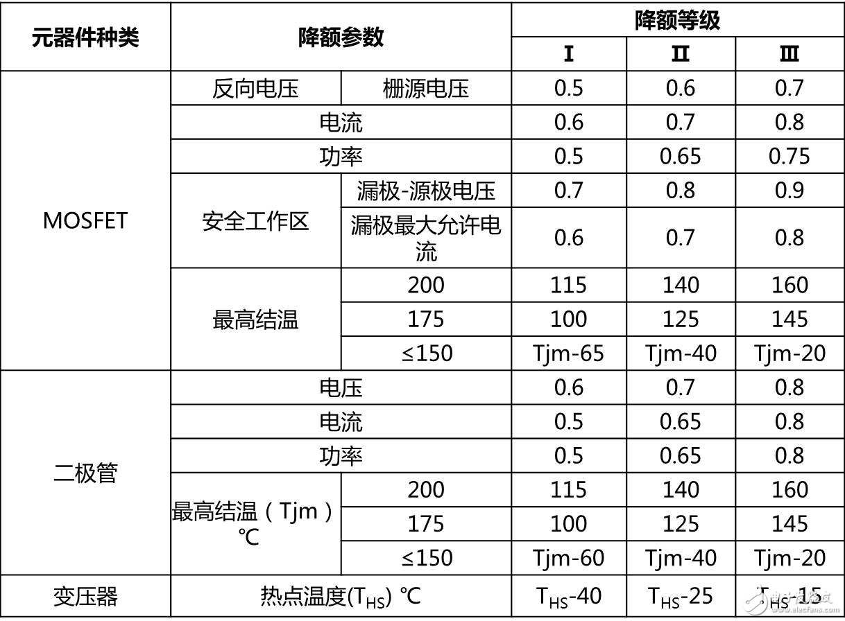
The derating design is to derate the components, that is, the working stress of the electronic components is properly lower than the specified rating, and the derating device can delay and reduce the degradation, thereby improving the reliability of the device. It also improves the reliability of the module. The failure rate of electronic components is sensitive to voltage stress, current stress and temperature stress, so the derating design is mainly for these three aspects. The derating level of electronic components can refer to "National Military Standards - Component Derating Guidelines GJB/Z35-93", which can be generally divided into three derating levels:
(1) Level I derating: Level I derating is the largest derating, which applies to equipment failures that will endanger safety, resulting in mission failures and serious economic losses.
(2) Level II derating: The reduction of working stress has obvious benefits for the reliability growth of components. It is suitable for equipment failures to degrade work tasks or to pay unreasonable maintenance costs.
(3) Level III derating: Level III derating is the minimum derating, and component costs are relatively low. Applicable to equipment failures has only a small impact on the completion of work tasks, or can be repaired quickly and economically.
The following table shows the derating parameters for some of the key components commonly used in power modules:

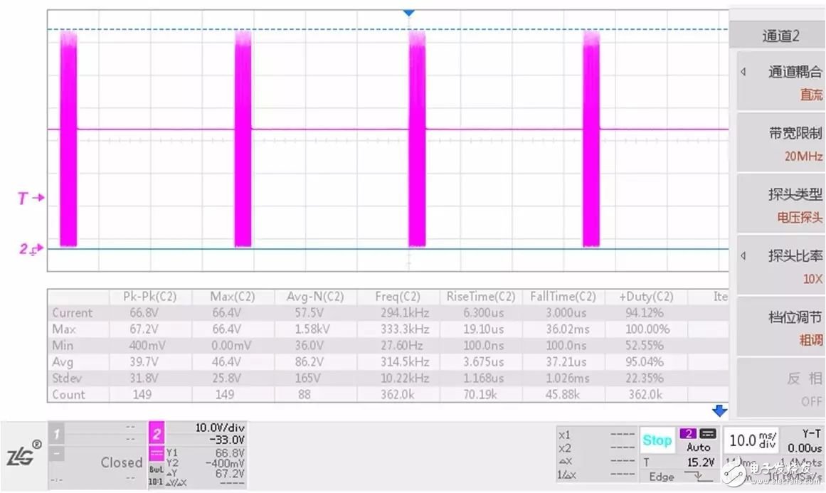
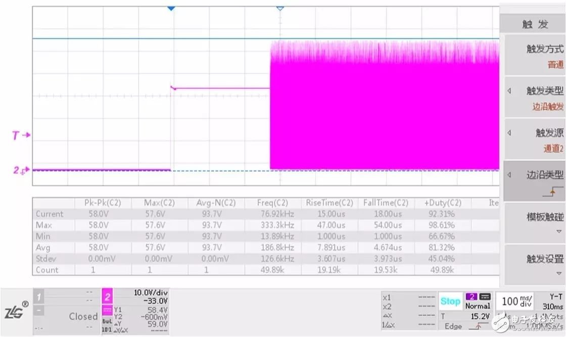
For the stress design of the power module, focus on the field effect transistor (MOS transistor), diode, transformer, power inductor, electrolytic capacitor, current limiting resistor and so on. It can guarantee sufficient derating under various limit conditions such as steady state, transient and short circuit in the whole voltage range to ensure the reliability of the product. For example, for a MOS tube with a maximum Vds voltage of 100V, as the main power switch tube of the power module, the various states under the highest input voltage are measured (as shown in Figures 1-3), the highest Vds=67.2V, derating The factor is 0.672, which meets the level I derating, and the margin is sufficient.

Figure 1 MOS tube waveform Vds_max=57.2V during steady-state operation

Figure 2 MOS tube waveform Vds_max=67.2V when output short circuit

Figure 3 MOS tube waveform Vds_max=59V during start-up transient
As the power module becomes smaller and smaller, the power density is correspondingly higher and higher, and the problems related to the thermal design of the power module are particularly prominent. Especially for the power module using electrolytic capacitors, the high temperature will accelerate the consumption of the electrolyte of the electrolytic capacitor, greatly reducing the life of the electrolytic capacitor. The high temperature will accelerate the aging of the component materials, for example, the insulation properties of the transformer enameled wire are lowered, resulting in poor insulation withstand voltage or even short circuit between turns. Therefore, a good thermal design not only extends the service life of the power module and its surrounding components, but also makes the entire product heat evenly and reduces the occurrence of faults.
The basic task of the thermal design of the power module is to reduce the heat generated inside the module as much as possible by the thermal design to meet the performance requirements, reduce the thermal resistance, and choose a reasonable cooling method. Heated components should be dispersed as much as possible. When designing the PCB board, the current carrying capacity of the printed wiring should be ensured. The width of the printed wiring must be suitable for the conduction of current. For high-power chip components, a large area of ​​copper foil can be used to increase the heat dissipation area of ​​the PCB. The inside of the power module can be filled with thermal silica gel and resin to reduce the temperature rise of the internal components of the module. For larger power modules, heat sinks can be used to dissipate heat, increasing the surface area of ​​convection and radiation, which greatly improves the heat dissipation of the electronics.
For power modules that have not been potted, an infrared thermal imager can be used to "face" the entire power module. The infrared thermal imager converts the invisible infrared energy emitted by the object into a visible thermal image. The different colors above the thermal image represent the different temperatures of the object being measured. Then, after analysis, the thermocouple is used together with the data acquisition equipment to focus on the "point" temperature measurement of the key components of the MOS tube, rectifier diode, and transformer isothermal rise. From face to point, rigorous testing to ensure that the temperature derating of components meets the requirements.

Figure 4 Thermal imaging diagram of a power module at normal temperature
For example, for a power module, the surface temperature of the power module is tested by an infrared thermal imager after working for a long time as shown in Fig. 4. The maximum temperature of the MOS tube at normal temperature and not potted is 85.5 °C, and then the thermocouple is used with the data acquisition instrument. The filled potting compound is tested under various conditions for a temperature of up to 97.2 ° C. For a MOS tube with a maximum temperature of 175 ° C, the temperature derating satisfies the I-level derating.
Therefore, in addition to the basic performance parameter test, comprehensive high and low temperature test, electrical stress and thermal stress test, to ensure sufficient derating design requirements, and through long-term aging test, can judge whether the power module is safe and reliable. The power modules independently developed by ZLG Zhiyuan Electronics are all designed with strict derating design and comprehensive high and low temperature tests. The performance and reliability of the products are adequately guaranteed. For example, the above example is part of the test data of a model of ZLG Zhiyuan Electronics E_UHBD-15W series. This series of products has wide input voltage range, high efficiency, low temperature rise, stable and reliable, and is widely used in industrial control, power, communication, medical , instrumentation and automotive electronics and many other fields.
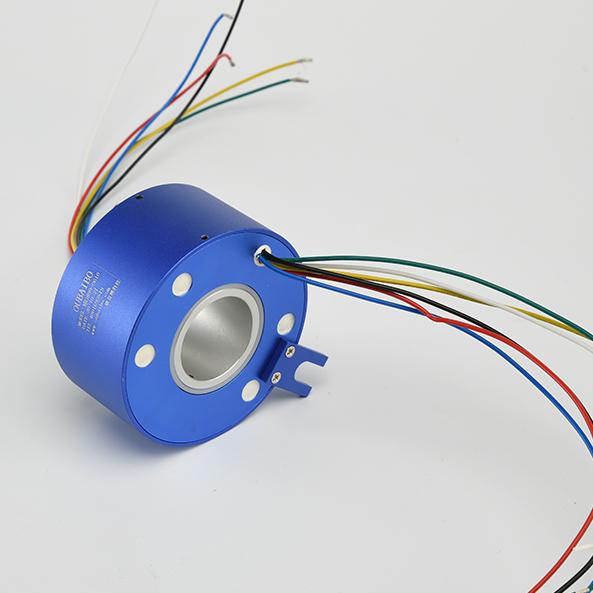
A through-bore slip ring is an electrical device that allows current to pass between two points in a rotating assembly without a physical connection. There is no break in the circuit. This is accomplished by passing the current through a rotating brush that contacts a stationary metal ring. The metal ring is mounted on the shaft of the assembly and provides a continuous path for the current.

It is an integrated circuit component that consists of two conducting rings that are separated by a gap or spacer. When the rings are brought into contact, current can flow between them and produce a rotational motion. Slip rings are used in various applications where high efficiency and low power consumption are essential, such as communication systems, motor control systems, and energy harvesting devices.
The through-bore design allows for rotation of the assembly while transmitting power or data. They are often used in applications where there is a need to rotate an object while keeping a power or data connection open, such as on a wind turbine or radar antenna.
The Oubaibo's through-bore slip ring is a newly designed product that has many advantages over other products on the market. It is small and lightweight, making it easy to install and use. The through-bore design also allows for a high degree of flexibility, making it ideal for use in difficult or tight spaces. Additionally, the Oubaibo through-bore slip ring is very efficient, providing a high degree of power transfer with minimal loss.
Through-Bore Slip Ring,Slip Ring Connector,Power Slip Ring,Slip Ring Assembly
Dongguan Oubaibo Technology Co., Ltd. , https://www.sliproubo.com
