High-impedance signal measurements such as air quality detection, photoelectric signal detection, accelerometers, piezoelectric sensors, and biological signals are susceptible to input resistance and input bias currents from the measurement system. The actual measurement system is mainly parallel to the signal path. Components such as shunting of resistors and capacitors, cable leakage currents, and parasitic leakage currents on printed circuit boards. Therefore, the high-impedance weak signal measurement circuit must be carefully designed to meet the system's requirements for low bias current, low noise, and high gain.
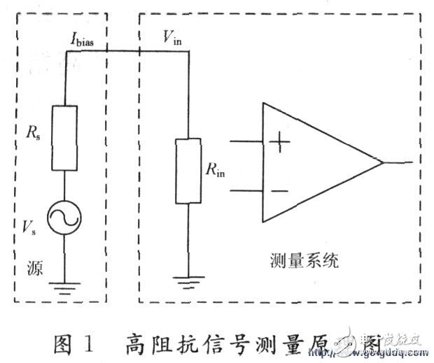
1 High-impedance signal measurement principle and influence factor analysis High-impedance signal measurement is susceptible to the partial pressure of the input impedance of the measurement system and the system input bias current. As shown in Figure 1, the measured high impedance signal source is connected to the measurement system. The Thevenin equivalent circuit of the signal source is formed by connecting Vs and Rs in series. Assuming that the equivalent input resistance of the measurement system is Rin and the input voltage is Vin, due to the partial pressure of Rs and Rin, the input voltage is reduced, and the input voltage of the measurement system is:

Assume Rs=1 MΩ and Rin=100 MΩ. When Vs=1 V, Vin=O. 99 V, it can be seen that the load effect of the system input resistor produces a 1% error. To achieve high-precision measurement, you need to increase the input impedance of the measurement system.
As shown in Figure 1, the bias current of the measurement system is Ibias. Assume that the positive current is flowing into the measurement system. This current will produce an error voltage on the source resistance Rs. The input voltage detected by the actual measurement system is:

0.99 V. At this point, the input bias current will cause a 1% error. To achieve high-precision measurements, you need to reduce the input bias current of the measurement system.
From the above analysis, it can be concluded that increasing the input impedance of the measurement system and reducing the input bias current is of great significance for the measurement of high impedance signals. The input impedance of the measurement system should be much larger than the internal resistance of the measured signal source to meet the measurement accuracy requirements.
The equivalent input impedance of the actual measurement system mainly includes the signal cable insulation resistance, the shunt resistance of the signal conditioning circuit, the input impedance of the amplifier, and the parasitic resistance of the printed circuit board. The input bias current of the system mainly includes the shunt current of the signal conditioning circuit, the signal input cable, and the leakage current on the printed circuit board. Currently, high-input-impedance, low-noise FET amplifiers have input impedances as high as 1010 to 1012 Ω and input bias currents on the order of picoampere (pA). The voltage and current noise performance can meet universal applications. Since ideal high-value resistance and low leakage current capacitance are often difficult to obtain, the weak signal output from the sensor needs to undergo various conditioning before amplification. The design of the signal conditioning circuit is very important, which determines the measurement system. performance. How to improve the input impedance of the measurement system, reduce the input bias current and reduce the system noise have become the main factors for high-impedance weak signal detection. Here mainly to improve the system input impedance and reduce the input bias current for research and analysis.

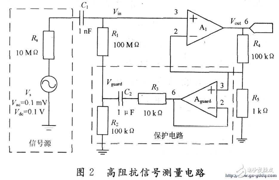
2 Circuit Design and Analysis The protection referred to here refers to a technique that approximates the potential of a low-impedance node potential in a circuit to the potential of a high-impedance input terminal, that is, through a low-impedance protection circuit, the low-impedance node in the circuit. The potential is forced to pull up to approximately the same potential as the high-impedance input. Here for the measured signal is the source resistance Rs = 10 MΩ, AC signal amplitude is O. 1 mV, high impedance weak AC voltage signal with a DC signal level of 0.1 V. The Thevenin equivalent circuit of the signal source is shown in the dashed box on the left side of FIG. 2 , and is composed of Vs and Rs in series. The signal conditioning circuit includes a high-pass filter circuit, a preamplifier circuit, and a protection circuit.
Due to the actual detection signal, the frequency components are often more complex, and sometimes the signal that you want to measure is deeply buried in the noise of other frequency signals. Therefore, the signal needs to be filtered before entering the amplifier. This circuit needs to measure the signal as an AC signal, which is masked by the DC level. Therefore, it needs to be filtered by the high-pass filter. The cutoff frequency of the filter is determined by the bandwidth of the measured signal. The cutoff frequency of the high-pass filter is changed by changing the values ​​of C1 and R1. It should be noted that, theoretically, the greater the resistance of the resistor R1, the better, this can provide the input impedance of the measurement system, in fact, the resistance of large resistance is often not easy to get, here choose the resistance of 100 MΩ, Qualcomm The cutoff frequency is fH=1.6 Hz.
As shown in FIG. 2 , the pre-stage signal amplification circuit adopts a phase-comparison operation circuit structure. This circuit introduces voltage series negative feedback to increase the input resistance and reduce the output resistance. The amplification factor A is equal to:
A=1+R4/R5 (3)
As shown in Figure 2, the circuit resistance values ​​are: R4 = 100kΩ and R5 = 1kΩ, so the amplification factor is A=101. Here it is necessary to pay attention to the advantages of the high input resistance and low output resistance of the comparative arithmetic circuit. However, because the integrated op amp has a common mode input, an integrated operational amplifier with a high common mode rejection ratio should be used to improve the operation accuracy.

In the conventional method, the lower end of the resistor R1 is directly connected to ground. The input impedance of the system mainly depends on the value of the resistor R1, and the equivalent input impedance of the system is approximately equal to 100 MΩ. From the above analysis, it can be concluded that the measurement error will reach 10%. Such a large error is not allowed in practical applications. By designing the protection circuit, this problem can be well solved.
The circuit in the lower dashed box in Fig. 2 is a protection circuit. A signal is input from the inverting input of the amplifier A1 to the non-inverting input of the protection amplifier Aguard. The protection amplifier is actually a voltage follower. The low potential end of the resistor R1 is added with the guard potential Vguard when R2"R3. In a certain frequency range, the protection potential is approximately equal to the high-impedance input potential Vin, and the magnitude of the protection potential can be changed by adjusting the resistance of R2, R3. The protection potential is provided by the protection buffer amplifier instead of the signal source. After the low impedance end of the resistor R1 is added with the protection potential, the voltage drop will be greatly reduced, and the current flowing through it will also be greatly reduced.
The protection circuit needs to satisfy the impedance of the signal path much larger than the impedance of the protection circuit, that is:

Where: Zs represents the impedance of the signal path and Zg represents the impedance of the protection circuit. In this design, R2 = 100 kΩ, C2 = 1 μF, and Zs/Zg = 10,000.
In the measurement of high-impedance weak signals, the selection of the operational amplifier is crucial, and high input impedance, low input bias current, low noise, and other parameters need to be considered. The circuit uses AD743's extremely low noise BiFET operational amplifier, the AD743, which has a maximum input bias current of 250 pA, an input impedance of up to 1010Ω, and a CMRR of 90 dB.
In the actual measurement system, for the error caused by the input signal cable, the cable with the highest insulation resistance can be selected. In addition, adding the protection potential Vguard to the cable shield can greatly reduce the error caused by the cable leakage current. Printed circuit boards cause leakage currents due to a decrease in insulation resistance due to contamination, etc. When the op amp's non-inverting input is adjacent to the power input, it will cause interference. Therefore, the protection potential is loaded on the input side of the op amp and around the signal line. The leakage current on the signal path will be greatly reduced, and the leakage current from the power supply will be absorbed by the protection circuit.
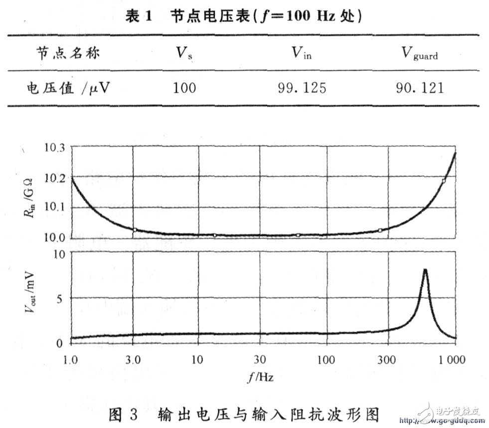
3 Simulation Results Analysis For the circuit shown in Figure 2, the circuit was simulated using PSpICe simulation software. The results of the AC scan are as follows. The voltage at each critical node is shown in Table 1. The low impedance end of resistor R1 is added with 90.121μV. For the protection voltage, the shunt current through resistor R1 is 90.031 fA.
As shown in Figure 3, the upper part of the figure shows the waveform of the system output signal, and the lower part shows the waveform of the system input impedance. From the figure, we can see that at the frequency of 100 Hz, the output voltage value Vout of the measurement system is 10. 011 mV, AC input impedance Rin is 1.132 8 GΩ. After calculation, the magnification of the system A is 100.998 times.

From the above analysis, it can be concluded that using the protection circuit greatly improves the input impedance of the system and reduces the input bias current of the system. The simulation results are in accordance with the theoretical analysis. The protection circuit provides high-precision measurement of high-impedance weak voltage signals.
4 Conclusion <br> This article starts from the principle of high-impedance signal measurement and analyzes the influence of the input impedance and bias current of the measurement system on the measurement accuracy. According to the high-impedance weak voltage signal, the protection technology is applied to design a high protection circuit. Impedance weak signal amplification circuit, through PSpice software simulation analysis, verified that this circuit can realize high-precision measurement of high-impedance signals, and provides a valuable reference method for high-impedance signal measurement.
Somke Machine
Fog Smoke Machine
Feature:
* DURABLE MATERIAL: It is made of top grade aluminum alloy, built-in fan for heat dissipation, stable and lightweight. Look upscale and durable for long time.
* BEAUTIFUL COLOR SHOW: It can choose single colors or color combinations. It will be great enjoyment to see the colorful light projected to the ceiling, wall and floor,etc.
* SUIT FOR VARIOUS OCCASION: Suit for various parties, birthday, dance, holiday, celebrations, Karaoke, family or friend home celebration. The laser light can be used in home, disco, living room, bar, club, or anywhere needed.
* EASY OPERATION: The light will enter sound activated mode, which makes the lights blink according to the beat of the music or sound. Adjustable motion speed.
* CREAT ATMOSPHERE EVERYWHERE: This laser light is mini size with tripod, portable and convenient for carry. You can place it everywhere.
Our company have 13 years experience of LED Display and Stage Lights , our company mainly produce Indoor Rental LED Display, Outdoor Rental LED Display, Transparent LED Display,Indoor Fixed Indoor LED Display, Outdoor Fixed LED Display, Poster LED Display , Dance LED Display ... In additional, we also produce stage lights, such as beam lights Series, moving head lights Series, LED Par Light Series and son on..
Somke Machine Series,Smoke Machine,Wedding Smoke Machine,Smoke Machine Party
Guangzhou Chengwen Photoelectric Technology co.,ltd , https://www.cwstagelight.com
