Abstract: This paper introduces the design and implementation process of digital communication experiment device for video signal with FPGA as the main control chip and optical port as communication medium, and explains the function and implementation of each module of the circuit. The circuit is designed in altium designer, adopting sub-module design, flexible ideas, clear structure and easy to implement. The VerilogHDL language is used to program and simulate the program in the Quartus II environment. The device has been made into a physical sample, and the experimental use shows that the transmission of the video signal can be realized, and the teaching requirements and practical effects proposed by the design can be achieved.
Keywords: FPGA; video signal; optical communication; VerilogHDL
Optical fiber has brought about reforms and innovations in the communication field with its advantages of frequency bandwidth, large capacity and low attenuation, forming an emerging industry. Compared with traditional analog communication, digital communication has the advantages of strong anti-interference ability, wide application range, strong security performance, easy integration and stable function. Digital fiber-optic communication has both advantages and will definitely become the development direction of the communication field.
The optical fiber transmission of video signals has the advantages of real-time, accurate and clear. In the field of experiments, experimental images can be transmitted quickly and accurately, giving the experimenter more reliable information. In terms of monitoring, the monitoring image can be transmitted in real time, which saves cost and has high transmission quality. Therefore, the research and implementation of optical fiber transmission of video signals will facilitate people's study, work and life.
This paper is aimed at the general engineering and engineering colleges, non-communication and information engineering majors, and has developed innovative experimental teaching instruments developed by popular experimental teaching subjects. The introduction of the experimental instrument is conducive to the promotion of the experimental courses of basic subjects in colleges and universities, enriching and perfecting the content of the experimental courses, so that students can understand the development of modern technology and the mastery of relevant knowledge.
1 System hardware structure The whole device consists of two parts: the light receiver and the light emitter. The two are connected by fiber optics. The light emitter is related to the working principle of the light receiving ,, one is the reverse process of the other; the light emitter converts the electrical signal of the video into an optical signal, and the optical receiver converts the optical signal into an electrical signal of the video.
The light emitter is composed of filter amplification, A/D conversion, control part, parallel/serial conversion, and electric/optical module parts.
The optical receiver is composed of an optical/electrical conversion section, a serial/parallel conversion, a control section, a D/A conversion, and an analog signal amplification section.
2 system circuit design
2.1 Power Supply The whole device is only powered by 7.5 V DC power supply. The internal integrated circuit needs to use 5V, 1.5V, 3.3V power supply. The 5V power supply is provided by the L7805 tri-state regulated power supply, and 3.3V and 1.5V are provided by ASM117-3.3 and ASM117-1.5, respectively.
2. 2 FPGA main control part The circuit adopts the model EPIC3144C8 FPGA as the main control chip, and the working clock is provided by the 32 MHz crystal oscillator. The chip has four clock inputs, one of which is the input crystal clock. Since each module of the FPGA is used, each module needs to be powered and grounded.
There are two phase-locked loops inside the FPGA, which can be divided and multiplied to get different frequencies. The FPGA in the transmitter provides the clock of the analog-to-digital conversion chip and the parallel/serial conversion chip and encodes the eight-bit data outputted by the analog-to-digital converter into ten-bit data to be transmitted to the parallel-serial conversion chip, that is, the 8B10B encoding and data transmission are completed. The FPGA in the receiver provides the digital-to-analog converter operating clock and the reference clock of the serial-to-parallel converter, and decodes the tens of bits of the serial-to-parallel converter output and restores it to eight-bit data to the digital-to-analog converter. The function of the FPGA is implemented by Verilog programming, and the program is downloaded to the FPGA using the AS (active) configuration.
2.3 Processing and Acquisition of Video Signals Video signals are filtered, amplified, and separated by synchronization. The analog-to-digital conversion integrated chip collects and converts them into digital signals.
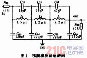
2.3.1 Filtering amplifying part When sampling a video signal, when the signal contains more than one-half of the sampling frequency, if the sampling frequency is not high enough, an aliasing signal will be generated. Aliased signals cannot be removed by digital filtering and require hardware filtering. The sampling frequency of the A/D conversion needs to be higher than 2 to 10 times of the highest frequency of the video signal. In order to prevent higher frequency from occurring during the analog to digital conversion phase, that is, no aliasing interference signal occurs, the filtering needs to be performed before the A/D conversion. According to the bandwidth of the desired video signal and the characteristics required for anti-aliasing filtering, a 7-stage low-pass filter is designed with a cutoff frequency of 6 MHz. The circuit is shown in Figure 1.
This article refers to the address: http://
The amplifier circuit is realized by the integrated AD8042 produced by American Analog Devices. The AD8042 is a low power, voltage feedback high speed amplifier. It has a single-supply capability with a 0.1BD gain flatness of 14 MHz and a differential gain and phase error of 0.04% and 0.06% with a 5 V supply, respectively. It operates with a bandwidth of 160 MHz when operating from a 5 V supply. Low distortion and fast settling characteristics make it suitable for buffering single-supply and high-speed digital-to-analog conversion circuits. The circuit is shown in Figure 2.
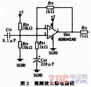
In the figure, the AD8042 is powered by a 5 V power supply and is amplified in one stage.
2.3.2 Synchronous separation part of the whole TV signal, in addition to the image signal, also contains a composite synchronization signal: composed of line, field and color subcarriers; these synchronization signals and image and sound signals are compiled according to international standards of certain specifications. The standard composition makes the entire video signal completely coordinated. Therefore, when performing the transmission processing of the video signal, the technical separation of the synchronization signal is performed to control the processing accordingly, and the specific circuit is implemented by using the LM1881 integrated chip. The chip extracts and separates image information from the full TV signal: line and field, delay synchronization, and odd and even fields. The composite video signal of the image is directly provided by the relevant equipment of the system. The BACK PORCH pin of the chip generates a post-pulse pulse during the blanking of the video signal. The pin is connected to the CLAMP port of the A/D converter AD9280, which is 19 feet, so that A/ The D converter is in the clamp mode during the blanking period of the signal, and can clamp the blanking level to the 0 level position, so that the timing relationship and the logical relationship between the signals can be correctly grasped when the processing signal is collected. Complete the function of synchronizing signal separation.
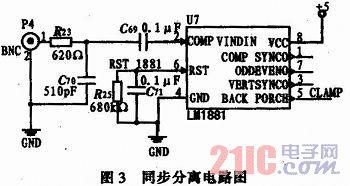
The separation circuit is realized by the integrated LM1881 produced by National Semiconductor Devices, and the circuit is shown in Figure 3.
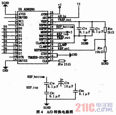
2.3.3 A/D Conversion Section The analog-to-digital conversion circuit is also implemented by the integrated AD9280 from Analog Devices, Inc., and its operating clock frequency is set to 32 MHz, which is provided by the FPGA. The signal is input by the AIN pin, and D0 to D7 output the converted 8-bit binary data. The STBY and THREE-STATE pins are grounded to ensure proper operation of the chip. CLAPMIN is grounded, and the blanking level is clamped to 0 level. The circuit is shown in Figure 4.
2.4 Signal transmission part The data processed by the FPGA is transmitted through the optical fiber. It is not necessary to convert the parallel data into serial data first, and then convert the serial data into an optical signal.
2.4.1 parallel/serial conversion circuit is realized by serializer DS92LV1023 integrated chip, the circuit is shown in Figure 5, and its corresponding receiving end is completed by the deserializer DS92LV1224 integrated chip. The DS92LV1023 converts 10-bit parallel data into a serial differential data stream that can be restored from the DS92LV1224 to 10-bit parallel data. This set of chips has a phase-locked loop inside, which can output its own matching clock for data output. The serializer LV1023 reference clock is selected as 32MHz, data is input at the clock frequency, and the internal matching of the chip generates a data output clock, and each 10-bit parallel data is converted into 12-bit serial data, wherein one start bit and one extra The stop bit, so the effective frequency is 320 M. The deserializer's reference clock is set to 16MHz to meet the data transmission needs.
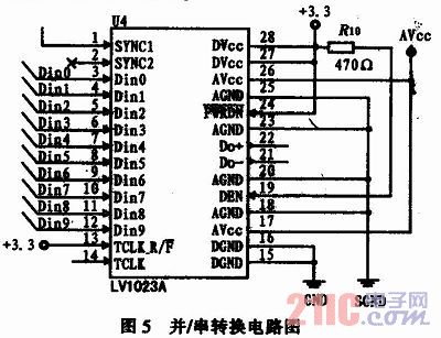
Since the video signal is continuous in real time, the generated data stream is continuously performed, so the circuit cannot be set to enter the high impedance state or the power saving mode, so the DEN and PWRDN of the LV1023 are set to a high potential.
The accurate transmission of serial data requires synchronization between the serializer and the deserializer. The set of chips has two synchronization modes:
1) The fast sync serializer LV1023 sends a set of sync signals consisting of six "1"s and six "0"s in succession. The transmit sync signal is controlled by SYNC1 and SYNC2. When SYNC1 or SYNC2 is set high, it continues. When the time exceeds 6 clock cycles, the synchronous signal is continuously sent. When the deserializer LV1224 receives the synchronization signal, it starts to try to lock the clock signal. Before the lock is completed, the LOCK remains high. After the lock is completed, the LOCK jumps to low power. level.
2) Random Synchronization Mode The chip can still be locked without synchronous signal transmission, which makes the chip available in open applications. In random synchronization, the serializer does not send a synchronization signal, and the deserializer directly locks the differential data stream. The locking mode is affected by the phase of the initial data and clock, and is also affected by the data itself, when a special data When the pattern reappears, the deserializer may have a locking error called RMT. But when the synchronization is lost, the deserializer will relock the clock and resume synchronization.
Because the circuit uses random synchronization. The serializer's SYNC1 and SYNC2 are left floating.
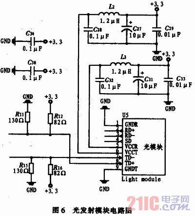
2. 4. 2 Electric/Optical Module The single-fiber bidirectional integrated transceiver module with the working mode of HNMS-XEMC41XSC20 and working wavelength of T1310nm/R1550nm converts the differential data stream of electrical signal into optical data signal flow. The circuit is shown in Figure 6.
2.5 Signal reception and processing
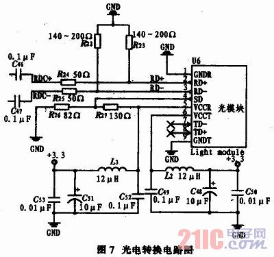
2.5.1 Optical/Electric Conversion Module The device transmits signals in a single fiber. After the optical signal is transmitted to the receiving device, it needs to be restored to an electrical signal, that is, a differential voltage data stream. The single-fiber bidirectional integrated transceiver module with the model HNMS-XEMC41XSC20 and working wavelength of T1310 nm/R1550 nm converts the optical signal into an electrical signal. The converted differential signal is output by RD+ and RD-. The circuit is shown in Figure 7.
2. 5. 2 Serial-to-parallel conversion The device uses the deserializer DS92LV1224 that matches the serializer DS92LV1023 in the transmitter. The serializer in the transmitter converts 10-bit parallel data into a serial differential data stream, so the corresponding differential deserializer is used in the receiver to restore the serial differential data stream to parallel data.
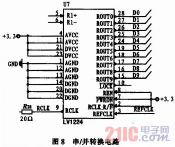
The DS92LV1224 has a phase-locked loop inside. When receiving a data stream, it can match the receiving clock according to the frequency of the data. The outside world only needs to provide a reference clock. The reference clock here is chosen to be 16MHz and is provided by the FPGA Control section. The chip also matches the clock synchronized with the deserialized data to facilitate parallel data output after conversion. The reference clock and data output clocks are the REFCLK and RCLK pins, respectively. In order to ensure the continuity and real-time performance of the video signal, it is necessary to avoid the chip in the power saving mode or the high resistance mode. Therefore, PWRDN and REN need to be connected to a high level. RCLK-R/F is connected to the high level, that is, the clock rising edge is selected to output data.
The chipset has two synchronization modes: fast sync and random sync. Fast synchronization is a synchronization signal sent by a serializer consisting of six consecutive "1"s and "0"s. The deserializer locks the data clock after receiving the signal. The LOCK remains high before the lock is completed. After the synchronization is completed. Jump to low level. The synchronization signal is sent by the SYNC1 and SYNC2 of the serializer. As long as either of them is set high for more than 6 clock cycles, the serializer starts transmitting the synchronization signal continuously. Fast synchronization has the advantage of being fast and accurate, but in long-distance signal transmission, the fiber only transmits data, and the SYNC and LOCK signals of the serializer and deserializer are not well transmitted. Therefore, random synchronization is adopted. The random synchronous mode serializer does not need to send a synchronization signal, and the deserializer directly locks the data stream to achieve synchronization. After the lock is lost, the deserializer will relock the clock. Connect LOCK to the FPGA for real-time control. The serial/parallel conversion circuit is shown in Figure 8.
2.6 D/A conversion and video signal output
2.6.1 The D/A conversion part adopts the AD9708 from Analog Devices, Inc., which is a high-performance, low-power CMOS digital-to-analog converter that provides excellent AC and DC performance and supports updates up to 125 Mz/s. rate. The operating clock is set to 16 MHz and is provided by the FPGA.
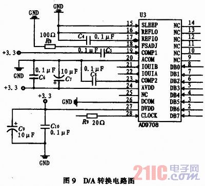
The peripheral circuit of the AD9708 is shown in Figure 9. Where REFLO is the reference ground for the conversion reference, this pin is grounded to disable the internal reference voltage. COMP1 is the noise attenuation mode setting terminal, where a 0.1 μF capacitor can be connected in series to achieve a better conversion effect. R9 is a termination matching resistor to eliminate high frequency oscillations. C9 and C10 are used to filter out digital power supply ripple, and C6 and C7 are used to filter out analog power supply ripple. Parallel data is input from DB0 to DB7, and the converted data is output by IOUTA. The signal output here must be amplified by the op amp to meet the technical requirements of the universal video display.
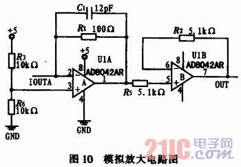
2.6.2 Analog Amplification and Video Signal Output The AD8042 is used to amplify the signal, as shown in Figure 10. The ULA converts the current signal output by the AD9708 into a voltage signal, where C1 is primarily used to remove high frequency interference. The ULB acts as a voltage follower for impedance matching. The required output impedance is 75 Ω, the voltage follower makes the output impedance 0, and then a 75 Ω series (not shown in the figure after the 7 feet of ULB) to meet the matching requirements.
3 Programming and Simulation The system is written in VerilogHDL language and edited in Quartus II environment. The FPGA internal clock is provided by a 32 MHz crystal. The work of the FPGA is as follows: 1) The working clock of the D/A converter chip AD9708, the A/D converter chip AD9280, the parallel-serial conversion chip LV1023, and the reference clock of the serial-to-parallel conversion chip LV1224 are both 16 MHz; 2) the transmitting end pair The data is encoded by 8B10B, and the converted data is transmitted to the serializer; the receiving end obtains the serial and converted ten-bit data, performs decoding, restores to the eight-bit data before encoding, and transmits the decoded data to the number. Analog conversion chip.
3.1 8B10B codec 8B10B encoding is the encoding method commonly used in high-speed serial communication. The purpose of 8B10B encoding is to convert eight-bit data into 10-bit data and make "0" and "1" in the converted data stream. The balance of numbers avoids errors caused by excessive repetition of "0" or "1" during transmission, improves the performance of line transmission, facilitates the receiver to capture the synchronous clock more accurately, and adopts specific symbols. The receiving end can be made to align the symbols more accurately.
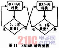
The 8B10B code can be regarded as a combination of 5B6B and 3B4B codes. Some codes may have two values ​​after combination. The difference between "1" and "0" is called balance, and RD- is used to indicate balance is +2 or 0. RD+ indicates a degree of balance of -2 or 0. The converted data is divided into two columns of RD- and RD+. Let variable DISPIN denote the balance of the number being converted, and DISPOUT denote the balance of the number of the next conversion. Initially, DISPIN is equal to DISPOUT, starting with RD-, if the number of converted "0" and "1" are equal, continue to convert the next number in the RD-column, if "0" and "1" If the number is not equal, go to the RD+ column to convert. Similarly, in the RD+ column, if "0" and "1" are equal, continue in RD+, otherwise switch to RD-.
The decoding portion decodes the first six bits and the last four bits of the 10-bit data according to the lists of 5B6B and 3B4B, respectively.
3.2 Simulation After the design program is successfully compiled by the Quartus II synthesizer, the input data, the data generated in the middle, and the output data can be simulated. The 8B10B encoding method adopted by the device is divided into 3B4B and 5B6B for encoding. The decoding section decodes the tens of bits of data into 4B and 6B, respectively, in accordance with the same distribution at the time of encoding. After decoding, they are combined into 8-bit data in order. The program is implemented by 4B3B and 6B5B respectively.

The program simulation diagram is shown in Figure 12. Adin is the eight-bit data before the encoding, and is set to count the data one by one. For convenience comparison, the graph is expressed in decimal. The encoded ten-bit data is data10b, and adout is the decoded data. It can be seen that although there is a delay, the decoded data is still count data. Therefore, the program can accurately implement the decoding function.
4 Conclusion In addition to the video signal, the full TV signal also includes the audio signal, and the transmission and conversion processing of the sound information is an indispensable content and complete in the application field. In addition to one-way communication, the transceivers exchange information with each other to realize two-way communication and complete reverse control functions, which are widely used and popularized in the field of optical fiber communication applications. The technical expansion and transformation of these topics, transplanted into the application of relevant experimental teaching, must have its positive role and significance.
FTTH Drop Cable Patch Cord,Plastic Box With Splitter,Wall Mounted Fiber Terminal Box
ShenZhen JunJin Technology Co.,Ltd , https://www.jjtcl.com
