1, background introduction
As various industries move toward the direction of intelligence, embedded products are increasingly demanding energy and efficiency. Especially in the smart grid, industrial and medical fields, the core MCU processor of a product faces multiple challenges. For example, an automated motor system or a distributed industrial system requires more digital signal processing capabilities to more precisely control the motor, and more and more advanced network interfaces (CAN, Ethernet or Wireless, etc.). ) to achieve real-time distributed monitoring or control functions. Another example is Figure 1. A solar inverter system requires a DSP engine to implement DC/AC or DC/DC algorithms. On the other hand, multiple inverters need to be connected to each other via Wireless or Ethernet Ethernet. Intelligent diagnosis and monitoring.
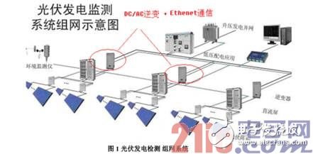
Faced with these needs, there are two traditional solutions that can be solved. One solution is to use two separate MCU/DSPs, one of which is used to implement digital signal processing or control algorithms, and the other MCU to implement a network protocol stack or graphical display interface. There are many shortcomings of this type of solution. First, two MCUs increase the PCB area, and the reliability and data throughput of the communication between the two MCUs are limited. In addition, the power consumption will also increase significantly, and the program developer even needs maintenance. Multiple hardware and software development environments. Another solution is to use a single core MCU/DSP with higher main frequency and more on-chip resources to perform data processing and auxiliary communication or display functions in a time-sharing manner. This solution significantly increases system cost and power consumption, the most deadly. However, when the customer's product needs to add new functions, the engineer needs to recalculate the resources of the MCU core and the running time required for different tasks, which requires more testing time, which is not conducive to expansion and product maintenance.
In the face of various deficiencies, heterogeneous dual-core architecture emerged as the times require, which can solve the above problems well. In fact, an asymmetric dual-core architecture MCU can allocate different system tasks to different MCU cores, with a fine division of labor and optimal balance of performance, power, and cost. Communication between the two MCU cores can be achieved in different ways, such as sharing memory areas and message areas, which is very simple and easy to implement. In the following sections, this article will use TI's latest Concerto series TMS320F28M35H52C as an example to elaborate on the advantages of asymmetric heterogeneous dual-core MCUs and their performance enhancements.
2, C2000 Concerto dual-core MCU features
The C2000 Concerto Series MCUs are TI's innovative heterogeneous dual-core products. The Concerto hybrid architecture delivers high performance, efficiency and reliability by integrating the industry's best real-time control and communication functions into one chip for real-time control loops and low-latency fast communication response [1]. The following describes its features from the kernel, memory architecture, communication peripherals and so on. The functional block diagram of the Concerto series TMS320F28M35H52C is shown in Figure 2 below.
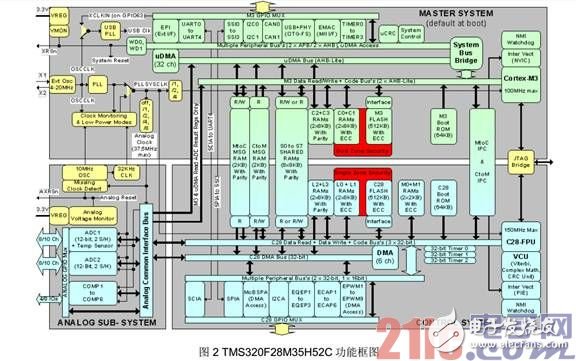
The first is a high-performance kernel. The Concerto Series MCUs include the Cortex-M3 and C28x cores. The Cortex-M3 core is the main system master subsystem core of Concerto, running at up to 125 MHz. The Cortex-M3 core is a 32-bit ARM core that is extremely cost-effective and has been widely used in the industry. Its performance and stability have been widely accepted by users, making it ideal for communication and event control. The C28x is a new generation of 32-bit DSP cores. It is the core of most of TI's existing C2000 products. It can run at up to 150 MHz. The C28x in Concerto has a floating-point unit (FloaTIng-Point Unit), VCU coprocessor, etc. , super performance, very suitable for large throughput data processing. The C28x acts as a Control subsystem and is macroscopically controlled by the Cortex-M3 Master subsystem.
This is followed by an optimized memory architecture. As shown in Figure 2, the C28x of the TMS320F28M35H52C can support 512KB of flash memory with ECC checksum, 64KB ROM, 36KB of RAM with ECC checksum, Cortex-M3 can support 512KB of flash memory with ECC checksum, 64KB ROM, 32KB ECC verified RAM [3]. Between the two cores is a shared peripheral and memory area. A total of 64K bytes of shared RAM, 4K of message RAM.
Once again, it is a peripheral. As shown in Figure 2, the T28320F28M35H52C's C28x core can control DMA, high-speed ADC (3MSPS), multi-channel high-precision PWM (24-channel PWM and 16-channel high-precision HRPWM), eCAP, eQEP, etc., which are optimized for closed-loop control. The Cortex-M3 core can support multiple serial communication interfaces, Ethernet, CAN and other industrial communication peripherals. At the same time, the two cores can share peripherals such as ADCs, enhancing the flexibility of the entire system.
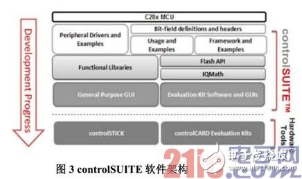
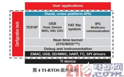
Finally, the software architecture. As shown in Figure 3, controlSUITE is a development resource and software package and development platform that integrates all C2000 MCUs. It provides peripheral routines, DSP libraries, documentation, and development board data for developers of TMS320F28M35H52C. ControlSUITE also offers a free full-featured real-time operating system TI-RTOS platform. As shown in Figure 4, TI-RTOS is based on the SYS/BIOS real-time kernel and integrates stable middleware such as TCP/IP protocol stack, USB protocol stack, FAT file system, IPC multi-core communication components, etc.
3. IPC inter-core communication
The communication between the Cortex-M3 and C28x cores accomplishes two major functions, one is data communication, and the other is the transfer of status and control information. IPC (inter-core communication) data communication requires a large amount of RAM to support, and information such as status and control requires only a series of status flags. In addition, the UART4 on the Cortex-M3 side and the SCIA on the C28x side; and the SSI3 on ​​the Cortex-M3 side and the SPIA on the C28x side are interconnected inside the Concerto. No hardware connection is required outside the chip, and CortexM3 is enabled for this type of function. System Configuration.
3.1 Message RAM memory area
The TMS320F28M35H52C uses Message RAM to implement IPC data communication. As shown in Figure 5, the 2K byte MTOC Message RAM is used to pass messages from the Master (Cortex-M3) subsystem to the Control (C28x) subsystem; the 2K byte CTOM Message RAM is used from the Control subsystem to the Master. The system delivers the message. Since both subsystems are equipped with DMA peripherals, the DMA can also read and write Message RAM, which increases system efficiency. The Message RAM area guarantees the exclusive access of Message through the read and write permissions of the RAM memory. For example, the C28x CPU and DMA can read and write access to the CTOM Message RAM area, while the Cortex-M3 CPU and uDMA can only read and access the CTOM Message RAM. Similarly, the read and write access rights of the two cores to the MTOC Message RAM area are reversed.

Message RAM is only used as a data buffer for IPC, and IPC is also done with the help of specific control logic. As shown in Figure 6, the Master subsystem and the Control subsystem implement IPC logic flow control through five registers: IPCACK, IPCSTS, IPCFLG, IPCCLR, and IPCSET. These five registers are all 32 bits, and each bit corresponds to one channel of the IPC, so up to 32 channels of handshake communication can be realized. A total of 4 channels from Bit0 to Bit3 can trigger the IPC interrupt of the message receiver. A total of 28 channels from Bit4 to Bit31 require a software query from the message receiver to obtain data in the Message RAM. If only state and control information (such as Semaphore in the RTOS) is passed between the two cores, only the above registers can be used without the involvement of the Message RAM.
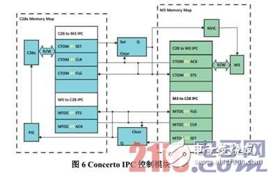
The following is a brief introduction to the operation flow of the IPC module by sending a frame of data to the Control subsystem by the Master subsystem.
1. Cortex-M3 first writes a frame of data in the MTOC Message RAM;
2. Cortex-M3 sets Bit9 of MTOCIPCSET (CM3 mapped memory area), as shown in Figure 6, where Bit9 of MTOCIPCSTS (C28x mapped memory area) will also be set;
3. C28x polls Bit9 of MTOCIPCSTS and queries that Bit9 is set. (If the previous operation is one of Bit0 to Bit3, C28x will be triggered to generate an IPC interrupt)
4. The C28x reads the data in the MTOC Message RAM. At this point, the Cortex-M3 successfully sends one frame of data to the C28x.
3.2 Shared RAM memory area
In most cases, the 2K byte IPC Message RAM area can satisfy the data communication between the C28x and M3 subsystems. With DMA, communication efficiency can be further improved. If the user wants to pass larger chunks of data in both subsystems at once, another way is through Shared RAM memory.
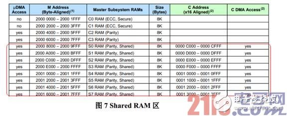
The TMS320F28M35H52C has a shared RAM area of ​​64K bytes, for a total of 8 S0-S7, each 8K bytes, as shown in Figure 7. The Cortex-M3 can be set to have any shared RAM area hosted by C28x or M3. For example, after mapping S0 to C28x side, C28x CPU and DMA can read and write S0, while M3 and uDMA can only read S0, can't write and Prefetching.
If the Cortex-M3 needs to send 6K bytes of data to the C28x side at a time, it can first map the Shared RAM area S0 to the local memory space, and then send a flag to the C28x via IPC to inform it that it can take the data away.
3.3 IPC Software Driver
Two IPC software driver libraries, IPC Driver and IPC_Lite Driver, are available in the controlSUITE software development kit. The IPC_Lite Driver uses only IPC registers for communication and does not require additional RAM, but the user can only support one IPC Interrupt Service ISR and does not support processing IPC requests in queue form. The IPC_Lite Driver is used as follows:
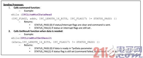
1. The kernel that initiates the data request will first call the name function provided by the IPC_Lite Driver. In this example summary, M3 is the kernel that sends the data and executes the "IPCLiteMtoCDataRead" function.
• IPC_FLAG2 is a C28 interrupt flag that indicates a message from the C28 core.
• IPC_FLAG17 is the response flag, which C28 uses to indicate that the M3 core has been processed.
• The address of C28 that needs to read data is also passed as a parameter to the C28 core.
• The reason this function is called in a while loop is that it may return STATUS_FAIL and will not send a message to C28 until MtoC IPC Interrupt 2 and Flag 17 are available, after which the function returns STATUS_PASS.
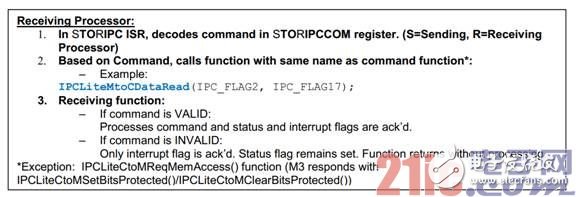
2. The kernel that passively receives the data request will parse the commands of its IPCCOM register in the ISR. In this example, the C28 MtoCIPCINT2 ISR knows that the flag is set, parses the command in the MTOCIPCCOM register, and recognizes that it is a read data command.
3. The kernel that passively receives the data request will call the same function name as the kernel that initiated the data request. In this example, C28 executes IPCLiteMtoCDataRead, IPC_FLAG2 as the interrupt flag parameter, and IPC_FLAG17 as the status flag parameter.
4. If the command is received, the IPC_Lite driver will process the read command and acknowledge the (acknowledges) status and interrupt flags. If the received command is invalid, then only the interrupt flag is acknowledged (acknowledged) to release the interrupt to subsequent commands, and the status flag is still set.
The IPC Driver creates a ring buffer in the Message RAM so that multiple IPC communication commands can be buffered in a queue and then processed one by one, and can support multiple IPC interrupt service routines ISR at the same time. Of course, the IPC Driver needs more. RAM to support. Unlike IPC-Lite, in order to use the IPC driver, some settings need to be added to the M3 and C28 projects.
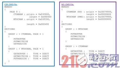
The first step is to add the IPC circular buffer and pointer segments to the CTOM and MTOC message RAM in the M3 and C28 link location files (.cmd). As follows:
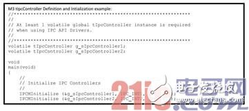
In the second step, at least one volatile global tIpcController variable (used for the C28 –M3 IPC interrupt) must be defined and initialized in the application source as follows:

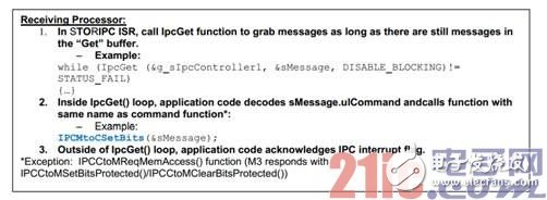
1. The kernel that initiates the data request will first call a command function provided by the IPC Driver. In this example, M3 is the kernel that initiated the data request and executes the "IPCMtoCSetBits" function.
• g_sIpcController1 is a variable of type tIpcController that controls communication between the M3 and C28 IPC interrupt channels.
• SETMASK_16BIT is a 16-bit mask indicating the bit field that should be set. IPC_LENGTH_16_BITS indicates that the data object for the command operation is 16-bits.
• The function is configured to allow blocking of "ENABLE BLOCKING", meaning that the function will wait until the M3 PutBuffer has an empty buffer. If the function is configured to block "DISABLE BLOCKING", it will immediately return STATUS_FAIL and will not send a message to C28 once the "Put" buffer is full. If the "Put" buffer has space, the function will return STATUS_PASS.
The message was successfully sent to C28.
2. The kernel that passively accepts data requests continuously calls the IpcGet function to read the messages in the sMessage structure, as long as there is a message in the "Get" buffer. In the ISR, the IpcGet function is called, and the tIpcController variable on the C28 side is used to bind the two IPC interrupt channels of the same M3 and C28 (the same as the tIpcController used to send commands on the M3 side).
3. Even if the kernel that passively receives data does not acknowledge (acknowledged) the IPC interrupt flag, the kernel that actively requests the data can still send messages continuously, because the tIpcController variable will queue the message to the "Put" buffer (with the kernel that passively receives the data request) The "Get" buffer is the same). The ISR of the kernel that passively receives the data request continuously fetches and processes the message until the "Get" buffer is
air.
4. Task division of the Cortex M3 and C28x cores
The strength of the Cortex-M3 subsystem is the ability to handle transactions and manage communication peripherals. The C28x core subsystem excels in real-time control and data processing. Therefore, in a system, it is crucial to properly allocate the processed transactions of the two subsystems and optimize the configuration of the resources. On the one hand, the Concerto-based system should maximize the advantages of the C28x DSP and real-time control, and take advantage of the closed-loop system composed of ADC, PWM, and C28x. On the other hand, the human-machine interface, communication protocol stack, and file system should be exhausted. May run on the side of the Cortex-M3 subsystem. The following two application cases discuss how to improve system efficiency through a reasonable division of tasks.
4.1 Photovoltaic inverter network node
The main function of the PV inverter is to invert the DC DC output from the PV panel to 110V/220V AC AC, and finally connect to the grid or off-grid to the power equipment. In a high-power photovoltaic network topology, there are often many PV inverters that need to be monitored. The control center needs to observe the working status of each PV inverter in real time. Therefore, the functions of the PV inverter network node mainly include DC/AC inverters and network connections. As shown in Figure 9, the C28x subsystem (running at 100MHz) completes the MPPT and DC/AC inversion algorithms. There are many ways to connect to the network. Common methods include Ethernet Ethernet, RS485 or CAN. The Cortex-M3 subsystem (100 MHz) of the TMS320F28M35H52C has interfaces such as Ethernet, RS485 and CAN, and supports a variety of wired and wireless connection functions.
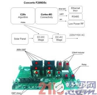
Figure 8 Solar HV DC-AC Kit
For the C28x subsystem, the design of the state machine is used to distinguish different system states. Different states represent different modes of operation, and other tasks can act accordingly depending on the particular mode of operation. For example, the following five different modes of operation are available.
• Power On Mode: After the system is powered on, it enters Power On Mode. After the system is powered on, the Cortex-M3 kernel boot program in the F28M35H52C1 is started first. At this time, the C28x control subsystem and the analog subsystem are in reset state, and the M3 main subsystem is required. It is released from the reset state. The M3 main subsystem sets the clock frequency of the M3 and C28x cores, since the ratio of the main frequencies of M3 and C28x must
It is an integer ratio, so the main frequency settings of M3 and C28x can only be 60/60MHz, 75/150MHz, 100/100MHz. After the M3 and C28x master frequency settings are completed, the M3 main subsystem needs to configure the peripheral resources of the entire chip and the GPIO to determine which GPIOs can be configured by the C28x control subsystem. The M3 and C28x frequencies in this system are set to 75/150MHz. When all initialization operations are completed, the system automatically transfers to Standby Mode.
• Standby Mode: All PWMs and relays are turned off. The system waits for a start command and also detects if an error has occurred.
• Soft Start Mode: Upon receiving the start command, the system enters soft start mode, and the PWM and relay are turned on. If the startup is successful and no error occurs, the system automatically enters the normal inverter mode.
• Normal Inverter Mode: The system outputs power in this mode. If no error occurs and the shutdown command is not received, the system will remain in this mode.
• Fault Mode: If an error occurs, such as a bus overvoltage, the system immediately enters Fault Mode. All PWM outputs are blocked and the output relays are disconnected. The Fault status can be cleared by a button or GUI. After clearing, the system will return to Standby Mode.
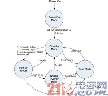
Figure 90 C28x end program system state machine
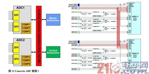
Figure 101 Concerto ADC block diagram
The Concerto series has two 12-bit ADC modules, each of which contains two sample-and-hold circuits, supporting synchronous or sequential sampling modes, and three analog comparators with 10-bit DACs. The input range of the analog signal is 0V~3.3V ( Internal reference) or VREFHI/VREFLO proportional relationship (external reference).
Figure 11 shows the detailed ADC configuration. The Cortex-M3 and C28x cores of the TMS320F28M35H52C have access to the ADC's result registers, and the two ADC modules share four analog inputs. This feature of the Concerto ADC module allows for critical signal security. Verify and improve system reliability.
4.2 Power Line Carrier Communication PLC Smart Home Gateway
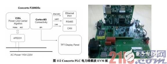
The smart home gateway can centrally manage the smart appliances in the room by wired or wireless. As shown in Figure 10, the T28320F28M35H52C's C28x (running at 150MHz) mainly completes the OFDM physical layer algorithm of the Power Line Carrier Communication PLC. The Cortex-M3 (75MHz) runs the TCP/IP protocol to access the Ethernet, and secondly, optionally through the UART interface to the external GPRS module or through the EBI expansion bus to connect to the TFT color screen user interface.
5, summary
The Concerto C2000 heterogeneous dual-core MCU combines the C28x DSP core with ARM's Cortex-M3 core to demonstrate the power of efficient data processing, data communication and event management. The two subsystems of the C28x and Cortex-M3 are clearly defined, and the IPC module intelligently realizes real-time and efficient inter-core communication. On the software side, the controlSUITE development platform offers a variety of components, including the TCP/IP protocol stack, IPC drivers, USB protocol stack, FAT file system, etc., to help users develop innovative products faster.
Ac Gear Motor,Ac Geared Motor,Asynchronous Ac Motor,Asynchronous Ac Gear Motor
NingBo BeiLun HengFeng Electromotor Manufacture Co.,Ltd. , https://www.hengfengmotor.com
