This paper introduces a novel miniaturized RF transceiver front-end design method. This method is used to implement an L-band dual-band RF transceiver front-end on the LTCC substrate. The circuit size is only 6.5 mm &TImes; 5mm &TImes; 0.5mm. The sample test results show that the performance indicators of the RF transceiver front-end have reached the expected design requirements, and have the advantages of low receiving loss, high transmission and reception isolation. The article introduces the working principle, detailed circuit design, three-dimensional structure realization, parameter simulation optimization to explain the whole design process in detail. Finally, the test results of the sample are simply analyzed in combination with the test curve.
With the development of modern wireless communication technology, the miniaturization of RF microwave devices and functional modules has become increasingly urgent. The L-band transceiver RF front-end described in this paper uses the LTCC process, which greatly reduces the circuit size by using the three-dimensional stacked structure of the passive circuit. In the circuit design, the use of a single λ/4 stub transmission and reception switching circuit not only ensures high transceiver isolation and low loss receiving circuit performance, but also saves a λ/4 stub than the traditional parallel switching circuit. The space occupied has reduced the circuit size.
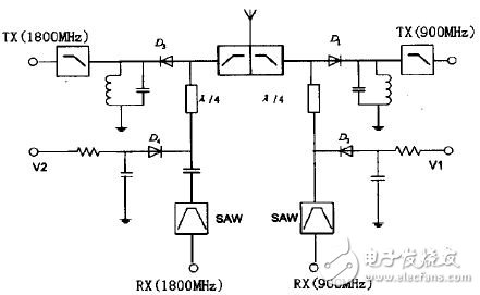
1 Working principleThe transceiver front-end described in this paper includes a 900MHz and 1800MHz duplexer, two PIN tube transceiver switches and two surface acoustic filters. The circuit principle is shown in Figure 1.

Figure 1 RF transceiver front-end schematic
2 circuit design2.1 Switch circuit design
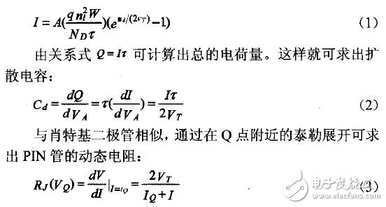
PIN diodes are often used as switching devices in RF microwave circuits. The structure is like a sandwich with an intrinsic I-layer or low-doped semiconductor inter-addition layer sandwiched between highly doped P+ and N+ layers. Let the thickness of layer I be W. Under forward bias, for a lightly doped N-type intrinsic layer, the current flowing through the PIN diode is:

The junction resistance and diffusion capacitance derived from the above formula can closely simulate the performance of a PIN diode in practical applications. The PIN tube is equivalent to the junction resistance Rs under positive bias (here, the positive bias is 2.5V, Rs is about 1 ohm); the reverse bias is equivalent to the diffusion capacitance CT (zero bias in this paper, CT about 0.5PF, The impedance below 2 GHz is 1000 ohms).
The λ/4 stub is often used for impedance matching between two networks in a narrow band. Let Z1 and Z2 be two unequal impedances, Z0 be the characteristic impedance of the transmission line, and adjust Z0 to satisfy:
Z20=Z1&TImes;Z2 (4)
Then a match is achieved between the two impedances. In Fig. 1, Z0 is known (50 ohms), and Z1 is the self-resonant impedance Rs when the PIN tube is positively biased or the open-circuit isolation impedance at the time of reverse bias. When the PIN tube is positively biased, Z1 is very close to the short circuit. After the λ/4 stub, it is equivalent to an open circuit at the common port, the receiving end is isolated, and the transmitting branch works. When the diode is reverse biased, Z1 is close to the open state (CT), and the transmitter is isolated to ensure low loss reception.
2.2 duplexer design
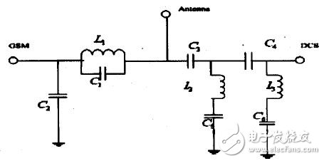
It can be seen from Fig. 1 that the signal received by the antenna is transmitted through a duplexer whose main function is to isolate the signals of the GSM900 band and the DCS1800 band. This article describes a GSM mobile phone front-end, the GSM band uplink and downlink frequency range is 890-915MHz (TX) and 935-960MHz (RX), DCS band uplink and downlink frequency range is 1710-1785 MHz (Tx) and 1805-l880MHz (Rx ). Figure 2 shows the circuit structure of the duplexer.

Figure 2 duplexer circuit diagram
As shown in Figure 2, there is a low-pass filter between the antenna and the GSM port. The cutoff frequency is around 1000MHz. C1 and L1 form a parallel resonance to generate the transmission zero. We design the resonance point around 1800MHz to suppress the DCS band signal. At the same time, it can increase the suppression of the second harmonic of the GSM band.
At the same time, there is a high-pass filter between the DCS port antennas. C5 and L2, L3 and C6 simultaneously generate series resonance, and the resonant frequency is around 900MHz, which is used to suppress the GSM band signal.
The transmit port low pass filter design can be done in the same way. Finally, the circuit simulation software designer of ansof company is used to simulate the whole circuit of the transceiver front-end module, optimize the parameters, and get an accurate circuit model.
3 three-dimensional structure realizationAfter the circuit simulation optimization design is completed, the appropriate passive components are modeled in the electromagnetic simulation software Q3D, and the C and L values ​​are optimized, and then the overall simulation optimization S parameters are introduced into the HFSS. For some components with large values ​​such as choke coils and current limiting resistors, it is difficult to implement LTCC due to the limitation of module substrate size and material dielectric constant. It is combined with nonlinear component PIN diode and surface acoustic wave filter (SAW). ) are attached to the substrate together. For the λ/4 stub, because the plane space of each layer is limited, it is realized by using multiple layers of spirals, which can save space and use it to generate capacitance to shorten the length of the λ/4 transmission line.
4 Experimental resultsThe final processed module is soldered to the test fixture for testing. The receiving insertion loss of both frequency bands is less than 1.9dB (the ripple within the passband is less than 0.5dB), and the transmission and isolation of both frequency bands are greater than 25dBc.
5 ConclusionThis paper introduces the design process of a miniaturized L-band RF transceiver front-end module, which is explained in detail from the aspects of circuit design, 3D modeling, simulation optimization and test result analysis. The single-section λ/4 stub transmission and reception switch circuit used therein effectively reduces the reception loss, improves the transmission and reception isolation, and reduces the circuit size, which is worth learning.
Fiber Optic Patch Cord,Fiber Patch Cord,Fiber Patch Cables,Fiber Optic Patch Cable
Huizhou Fibercan Industrial Co.Ltd , https://www.fibercannetworks.com
