Keywords: software radio, sigma-delta A / D converter, communication system?
1 Introduction Software radio is mainly composed of antenna, radio frequency front end, broadband A / D and D / A converter, digital signal processor (DSP) and various software. An important feature of the software radio architecture is to place A / D and D / A as close to the RF front end as possible. In order to reduce the analog link, at higher intermediate frequency, or even directly digitize the RF signal, all the functions behind are realized by software or digital hardware. The software radio communication system requires the ADC to have high speed, high precision, and wide-band input signal range.
The traditional ADC, which mainly relies on a resistor network to ensure quantization accuracy, cannot be made very accurate, and its high-end nonlinearity is inevitable. So, can we alleviate the dependence on the resistance network and rely on digital signal processing technology to improve accuracy? The answer is yes, but quantized in-band noise must be reduced. Thus, Σ-Δ ADC and Σ-Δ DAC came into being.
The essence of Σ-Δ A / D conversion technology is to reduce the complexity of the analog circuit as much as possible, reduce the quantization noise in the band, and then use a combination of digital signal processing and VLSI technology to improve the signal processing accuracy and increase the dynamic range. The Σ-Δ A / D conversion technology is discussed in detail below.
2 Σ-Δ A / D conversion technology?
2.1 The basic principle of Σ-Δ A / D converter?
2.2.1 Aliasing noise and quantization noise in A / D conversion
It is generally believed that the quantization noise of a traditional ADC can be approximated as follows: ![]()
Where q is the quantization step and b is the number of quantization bits. The corresponding noise spectral density is: ![]()
It can be seen that the more the number of quantization bits b, the lower the quantization noise power, the higher the sampling frequency fs, and the less noise is distributed in the baseband.
2.2.2 Basic principle of low-pass Σ-Δ A / D converter Low-pass Σ-Δ A / D quantization is developed on the basis of quantization. The block diagram of Σ-Δ ADC is shown in Figure 1. ?

The biggest difference between it and the traditional A / D converter is the quantization process. The latter has a one-to-one correspondence with sampling and quantization values, while the former almost completely abandons this point.
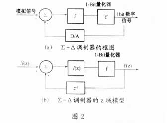
Figure 2 (a) is a block diagram of a typical sigma-delta low-pass modulator, and Figure 2 (b) is a Z-domain model of a sigma-delta low-pass modulator.

The difference between the analog signal to be quantized and the Σ-Δ modulated 1-bit output signal is sent to the integrator for 1-bit quantization, thereby obtaining a 1-bit stream with a sampling rate of fs. . Subsequently, the system sends the 1-bit stream to the subsequent digital decimator, which reconstructs a low-resolution high-resolution digital signal from these coarse quantized data. Because this method uses 1-bit quantization, the hardware structure is simple. Due to the high sampling frequency, the requirements for front-end analog anti-aliasing filters are greatly reduced. The two factors are the key to solving the difficulty of improving the resolution of traditional A / D converters. For traditional parallel A / D converters, each time the sampling frequency is doubled, the signal-to-noise ratio is improved by about 3dB, which is equivalent to 0.5 quantization bits. The sigma-delta converter is: every time the sampling frequency is doubled, the signal-to-noise ratio is improved by about 9dB, which is equivalent to 1.5 quantization bits. This means that to achieve a phase-quantized signal-to-noise ratio, the sigma-delta converter requires a much lower sampling rate than ordinary A / D converters.
In summary, the performance of the sigma-delta modulator is mainly due to oversampling, noise shaping and decimation.
(1) Oversampling Oversampling is a prerequisite for sigma-delta modulators to change accuracy with speed. The benefits of oversampling are: reduced quantization noise in the baseband. By formula (1), the noise power distributed in the baseband is: ![]()
Generally, fb≤fs, therefore, the noise energy in the baseband is greatly reduced. It should be noted that this is only the reduction of quantization noise caused by the increase in sampling rate fs excluding Σ-Δ modulation. If the quantization noise caused by Σ-Δ modulation is considered to move toward the high frequency side, the baseband noise power will be further reduced.
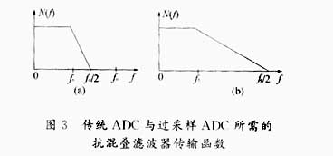
Another benefit of oversampling is that it reduces the requirements on the front-end anti-aliasing analog filter. The transfer functions of the anti-aliasing filter required by the conventional ADC and the oversampling ADC are shown in Figure 3 (a) and Figure 3 (b), respectively.

The transition band of the anti-aliasing filter of the traditional ADC is fn / 2-fb, and the transition band of the anti-aliasing filter of the oversampling ADC is fs / 2-fb, but fsfb. Traditional ADCs are much wider. Since the ratio of the transition band to the pass band determines the complexity of the filter, the requirements of the oversampling ADC for anti-aliasing filters are very simple. For example, for fs / fn = 64, a simple RC low-pass filter is sufficient.
(2) Noise shaping?
Noise shaping is the key to improving the output SNR (signal-to-noise ratio) of the sigma-delta modulator. The sigma-delta modulator can modulate low-frequency quantization noise to a high frequency band and change the noise distribution. This is the origin of noise shaping.
Noise shaping greatly increases the effect of oversampling, that is, the effect of increasing the working sampling frequency in exchange for quantization accuracy. Therefore, as long as the quantization noise outside the band is filtered, the speed can be effectively exchanged for accuracy from the 1-bit stream. This is why the sigma-delta converter achieves high resolution.
(3) Digital extraction?
Filtering the noise that will be folded into the baseband is the main task of the digital filtering stage. Removing the quantization noise is equivalent to improving the effective accuracy of the digital output, that is, reconstructing 1-bit data into multi-bit data. At the same time, it has to reduce the excessively high sampling rate.
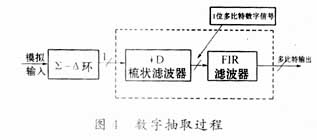
The output of the modulator is a coarse quantization of the analog input. However, the modulator samples at N times the Nyquist frequency. Therefore, high accuracy can be obtained by averaging these N points. The averaging process is equivalent to low-pass filtering in the frequency domain. The extraction process can be carried out according to Figure 4.

Using a single coefficient comb filter as the first stage of the decimator can greatly save time, but it can not effectively remove most of the out-of-band quantization noise. Therefore, in practice, an additional FIR digital filter is required. ?
In this way, the combination of oversampling, noise shaping and digital filtering methods can overcome the shortcomings of the existing VLSI technology that it is difficult to make analog circuits with small noise tolerance. Without additional processes, the use of low component accuracy and matching requirements Σ-Δ quantizer "to achieve high-resolution A / D conversion.
3 High-order Σ-Δ A / D conversion technology The baseband noise of the Σ-Δ A / D converter is much smaller than that of the Nyquist sampler or Δ modulator. However, for the aforementioned first-order sigma-delta modulator, the baseband noise cannot be reduced below the 60dB SNR requirement required by a 10-bit A / D converter. Therefore, to reduce the quantization noise in the baseband as much as possible, only the sampling frequency is increased. However, the increase in sampling frequency is limited by the operating frequency of the circuit and the performance of the digital filter. Accordingly, in order to increase the noise shaping effect in order to reduce the required sampling frequency, various high-order sigma-delta modulators have been developed based on the first-order sigma-delta modulator.
Next, we first discuss the second-order sigma-delta modulator. Since these stacked structures use a noise feed-forward solution, the system is always stable. When multiple first-order Σ-Δ loops are used together to obtain a higher-order modulator, the signal to the subsequent loop is the noise of the current loop. This noise is the difference between the integrator output and the quantizer output.
If the signals input to the second and third sigma-delta loops are Q1 and Q2, respectively, the quantized output of the second-stage sigma-delta modulator is: 
Similarly, for a 3rd order Σ? Δ modulator, 
Here, Q3 is the quantization noise of the third-stage sigma-delta modulator. ?
The analysis shows that the in-band quantization noise of the third-order sigma-delta modulator is significantly smaller than that of the first-order. ?
We used Matlab language to simulate the low-pass Σ-Δ A / D conversion process, and the results obtained are very consistent with the theoretical analysis (3rd order loop, output SINAD is about 108dB). The main procedures are omitted.
4 Conclusion Above, we made a more detailed analysis of the low-pass Σ-Δ A / D conversion technology. Foreign countries began to conduct large-scale research on Σ-Δ A / D and Σ-Δ D / A conversion technologies from the late 1980s. At present, there are mature Σ-Δ ADC and Σ-ΔDAC products.
references?
1 Edited by Yang Xiaoniu et al. Principles and Applications of Software Radio. Beijing: Electronic Industry Press, 2001?
2 Niu Xinxin and others. Software Radio Technology and Application. Beijing: Beijing University of Posts and Telecommunications Press, 2001
1.Shape:Conical ,Multi-pyramidal,Columniform,polygonal or conical
2.Material:steel plate.stainless steel compound plate,stainless steel plate,ect.(anticorrosion treatment with hot galvanization,also color polyester power could be coated on the surface)
High strength low alloy steel Q235,Q345,GR65,GR50 to ensure the mechanical properity of microelement in order to ensure the quality of galvanization (other materials are also avaliable on request)
3.Jointing of pole with insert mode,innerflange mode,face to face joint mode
4.Design of pole :against earthquake of 8 grade ,aganist wind pressure of 160
5.Minimum yield strength:355 mpa
6.Minimum ultimate tensile strength :490 mpa
7.Max ultimate tensilestrength:620 mpa
8.Certificate:ISO9001-2000
9.Length:Within 14m once forming without slip joint
10.Welding:It has past flaw testing.Internal and external double welding makes the welding beautiful in shape
11:Packages:Our poles as normal cover by Mat or straw bale at the top and bottom ,anyway also can following by client required , each 40HC or OT can loading how many pcs will calculation base on the client actually specification and data
Our lighting equipment are made from quality sheet from bending,forming,automatic welding and hot galvanization.We can reach one-run machining length of 14m,and can bend sheet thickness up to 25mm.We adopt advanced welding procedures ,automatically weld main joints and reach rank-II welding quality.

Galvanized Steel Pole,Galvanized Steel Electric Pole,Monopole Galvanized Steel Electric Pole,Galvanized Steel Street Lighting Poles
YIXING FUTAO METAL STRUCTURAL UNIT CO.,LTD( YIXING HONGSHENGYUAN ELECTRIC POWER FACILITIES CO.,LTD.) , http://www.chinasteelpole.com
