We know that our computer consists of three major components: CPU, memory, and hard disk. The CPU is used for calculation and control. The memory is used to temporarily store the data needed for running the program (loss of power-off data), while the hard disk is used to save the data for a long time (the power-down data is not lost).
The mobile phone we use every day is essentially a small mobile computer. It is also composed of three major components: CPU, memory, and storage devices. The storage device is equivalent to a computer's hard disk, which is used to store data on mobile phones for a long time, such as video, photos, music, and systems.
The hard disk of the computer has a mechanical hard disk (HDD) and a solid state hard disk (SSD). The former is a mechanical storage device and the storage medium is a magnetic disk. The latter is an electronic storage device and the storage medium is a flash memory. We cannot insert a mechanical device into a small cell phone, so the storage device on the cell phone can only be an electronic storage device, and the storage medium is also flash memory.
Now is the era of manpower and mobile phones. The mobile phone has become a part of people's body. Without a mobile phone in one day, it feels like something is missing and it is not fragrant to eat.

As a result, people’s demands for mobile phones are getting higher and higher: faster, more capacity, and smoother. In order to make mobile phones faster, mobile phone manufacturers use faster, more nuclear CPUs and increase system memory (4GB Not enough to use 6GB, 6GB is not enough to use 8GB), use faster storage devices. Whether it is a computer or a cell phone, the slowest running in a troika (CPU, memory, and storage device) is the storage device. The rapid advancement of the CPU and memory has driven the slowest storage devices to keep up with them, otherwise faster CPUs and large amounts of memory will make you feel uncomfortable with your phone.
In recent years, due to the application and development of flash memory technology, both hard drives on computers and storage devices in mobile phones have become faster and faster.
On the computer, from HDD to SSD, from SATA SSD to PCIe SSD, the hard disk is getting faster and faster;
On mobile phones, from SD cards, to eMMC cards, to UFS cards, the speed of memory cards is getting faster and faster. Now the general mobile phone is equipped with eMMC, and the flagship high-end mobile phone is equipped with UFS.
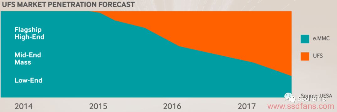
The protagonist UFS of our series has already appeared. Why UFS is the protagonist? Why do I have to take everyone to understand UFS? Because UFS will be the mainstream of mobile storage for a period of time in the future, we need to understand UFS and its related technologies.
So what is UFS? Universal Flash Storage, Universal Flash Storage. It has two meanings. One is the mobile phone storage interface protocol, similar to SATA, PCIe/NVMe; the other is the storage device that uses the protocol. Later articles appear UFS, the reader please understand according to the context.
Why UFS is the future of mobile storage? Without him, soon!
Everyone feels:

The latest UFS standard is UFS 3.0, which was released on January 30, 2018. Its maximum bandwidth can reach 2163MB/s! 4x SATA3.0 speed (600MB/s), exceeding PCIe3.0x2 speed (2GB/s unidirectional speed).
However, UFS products currently on the market are still UFS2.0/2.1, with a maximum bandwidth of 1081MB/s, which is also a spike-like SSD.
The UFS protocol was developed by the JEDEC() organization and was supported by companies such as Samsung, Hynix, and Toshiba. The following is the development history of UFS protocol:
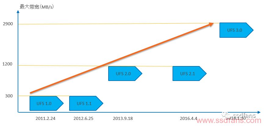
We can see that the UFS protocol has been striding toward higher and faster goals.
Why can UFS be so fast?
First, it uses differential serial transmission for data signal transmission. This is the basis of UFS fast. All high-speed transmission buses, such as SATA, PCIe, and SAS, are serial differential signals. Serial, you can use a faster clock (clock information can be embedded in the data stream); differential signal, that is, the level difference between the two signal lines represent 0 or 1. Compared with single-ended signal transmission, differential signals have strong anti-interference ability and can provide wider bandwidth (run faster). For example, suppose that the level difference between two signal lines represents 0 and 1. Specifically, the difference is greater than 0, indicating 1 and the difference is less than 0, indicating 0. If there is interference in the transmission process, interference levels of almost the same size are added to the two lines, the two are subtracted, and the difference is almost constant. Your uncle is still your uncle. But for single-ended signal transmission, it is very easy to be interfered with, for example, 0-1V means 0, 1-3V means 1 and a voltage of 0.8V originally, adding interference, becoming 1.5V, which means that 0 becomes 1 The data is wrong. Your aunt is no longer your aunt. Anti-interference ability, so you can use faster data transmission, which can provide a wider bandwidth.
The predecessor of UFS is eMMC, which uses parallel data transmission. The biggest problem with parallelism is speed, because once the clock goes up, the interference becomes larger and signal integrity cannot be guaranteed.
Second, UFS, like PCIe, supports multi-channel data transmission and currently supports up to two channels. Multiple channels allow UFS to choose between cost, power, and performance.
Also, it is a full-duplex mode of operation, that is, reading and writing can be parallel. Its predecessor, the eMMC, is half-duplex and cannot read and write at the same time.
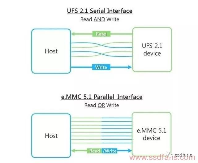
To make UFS fast, these infrastructures are a must. However, to make full use of the underlying high-speed data transmission channels, the upper layer data transmission protocol is also required. It's like we now have a spacious, flat highway. We need a high-speed car to drive on. If you let a tractor run on it, the highway is white.
How can the upper layer of the UFS protocol give full play to the advantages of the lower speed?
UFS supports command queuing, that is, the host can send many commands at a time, and then the UFS device supports parallel and out-of-order execution, and whoever finishes first returns the status. This command processing method is called asynchronous command processing. Its predecessor, eMMC, does not support command queues. Commands are executed one by one, or executed one by one. Each command has no execution. The following command cannot be sent. This command processing method is called synchronous command processing.
Let's compare the command processing modes and command execution efficiency of "full duplex + asynchronous command processing" and "half duplex + synchronous command processing".
• Half duplex + sync
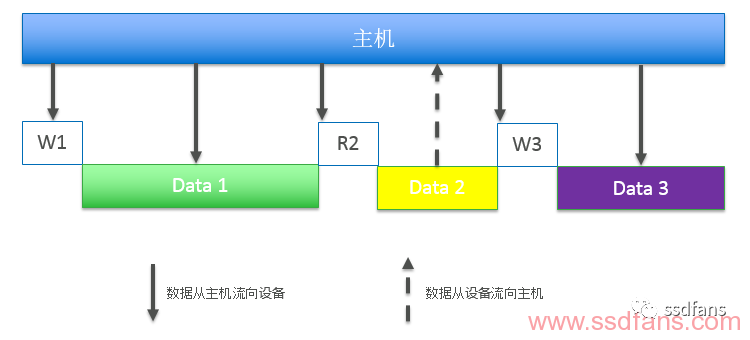
The host sends a write command W1 to the device, and then the host writes the data to the device; because it is a synchronous transfer mode, the command processing is handled one by one, so before issuing the read command R2, it must wait for the previous write command W1 to complete; Before sending the write command W3, you must wait for the R2 command to complete.
Full duplex + asynchronous
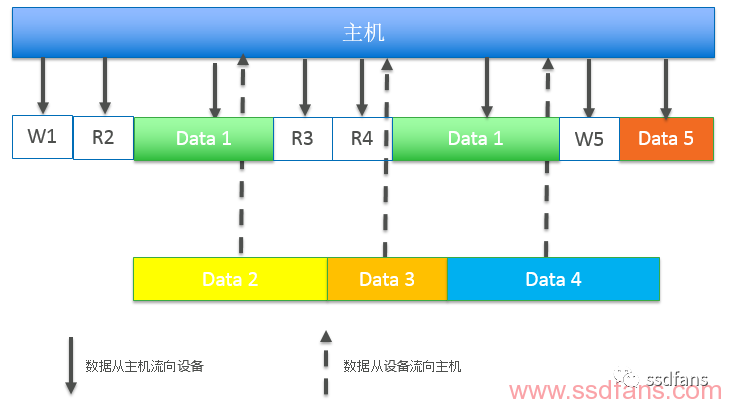
Since the command queue is supported, the host can send several commands to the device. As shown in the above figure, the host sends a write command W1 and read command R2 to the device. The device can process these two commands in parallel. Since the protocol supports full-duplex operation, the host can transmit the data of the write command W1 to the device, and the device can also return the data of the read command R2 to the host. The following commands R3, R4, W5... are similarly processed.
To put it another way, we compare the eMMC and UFS command execution methods with examples of moving goods:
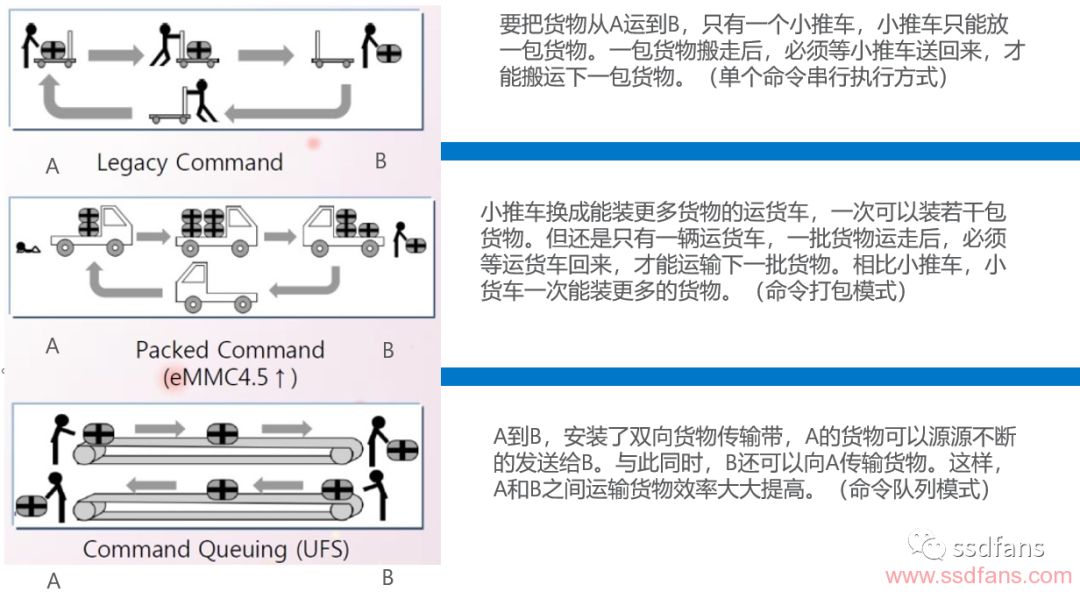
Nowadays, the mobile phone is very rich in applications. You have to listen to the song while you landlord and listen to the song. We must also talk about WeChat and multi-thread operations. Due to the presence of full-duplex and command queues, the efficiency of UFS processing commands is greatly improved, giving the user an excellent experience.
Earlier we took a few comparisons between UFS and eMMC, but I seem to forget to say that it is eMMC. Someone may be aggressive, what is eMMC?
eMMC, the Embedded Multi Media Card, is the mobile storage protocol developed by JEDEC. It is the UFS previous generation protocol standard.
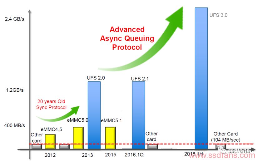
The latest eMMC standard is eMMC5.1 released in 2015. The maximum speed is 400MB/s. JEDEC already has UFS, and it is uncertain whether it will release a new eMMC standard. After all, the parallel transmission of eMMCs is limited by the physical signals and it is not realistic to expect a qualitative leap in speed.
As of this writing, I could not help but think of the events of last year.
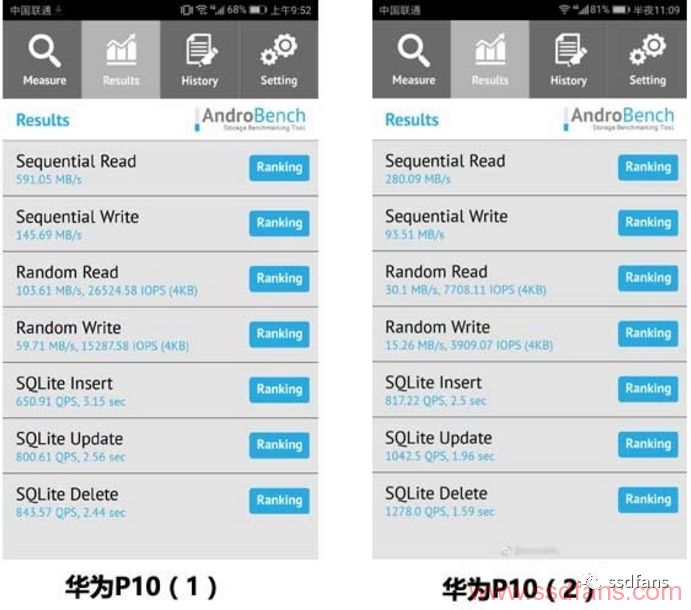
The same phone, some people UFS and eMMC mixed selling, the phone also sells a price, really no virtue! UFS and eMMC, speed difference is so great (see the figure below, from the network), the price can be the same? Can your system be further optimized to optimize eMMC sequential read/write speeds to 401MB/s? Do not pull any user experience, users are monkeys, and experience can be good? Water can carry a boat and it can also overturn it. Don't be too proud of it.
If eMMC is an HDD in a mobile phone, UFS is the SSD in the mobile phone. UFS replaces eMMC as the mainstream mobile storage protocol, which is no doubt. However, UFS has a stumbling block on the road leading up to the world, that is, NVMe. Some people say that NVMe is not an SSD protocol standard? That's right, but I want to remind everyone that Apple's current cell phone storage protocol is NVMe rather than UFS. In the short term, UFS and NVMe will exist in Android and iPhone respectively. In the long run, UFS and NVMe are two worlds, or combined, we can only wait and see.

Before the end of this chapter, give us a look at the physical map of UFS (BGA form):
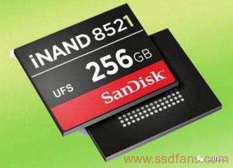
The size is like the thumb finger cover size. Small but complete. The UFS memory chip internally encapsulates the UFS controller and flash memory array, which is similar to the SSD structure. However, compared with SSDs, because of its smaller capacity, there are fewer flash dies and fewer flash memory channels. In addition, for power consumption and cost considerations, UFS chips are generally architectures without DRAM.
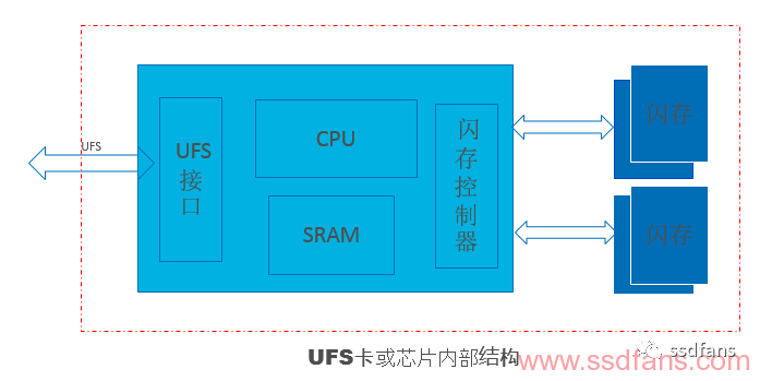
The internal design and implementation of the UFS chip is not the focus of our series. Subsequent articles in this series will focus on the UFS protocol.
A TPU Screen Protector made of the super toughness of the honeycomb structure. Its unique ultra-soft properties allow it to cover the most complex curves and contours in a device.
The self-healing design of the Hydrogel Screen Protector can protect the display screen of the device from damage, leave no air bubbles, and maintain the sensitivity of the touch screen. Advanced anti-fingerprint and dust- and oleophobic overlays keep your screen smudge- and dirt-free. This overlay is also important in providing maximum touch sensitivity for improved high-speed glide and optimal touch response.
The optical transparency of the Hydrogel Film is more than 90%, showing you the most original screen color and bringing the most realistic visual experience.
If you want to know more about the product information of the Hydrogel Screen Protector for Samsung, please click the product details to view the parameters, model, picture, price and other information of the Samsung Screen Protector.
Whether you are a group or an individual, we will do our best to provide you with accurate and comprehensive information about Hydrogel Screen Protectors!
Screen Protector For Samsung,Hydrogel Screen Protector for Samsung,TPU Screen Protector for Samsung,Hydrogel Film for Samsung
Shenzhen Jianjiantong Technology Co., Ltd. , https://www.jjtphonesticker.com
