There are many conventional methods for PCB layout, such as: hot spot dispersion; the device with the largest heat generation is placed at the optimal position for heat dissipation; the high heat dissipation device should minimize the thermal resistance between them when connected to the substrate; each layer of the PCB It is necessary to lay a large amount of copper and punch holes and so on. Before the PCB layout, the thermal design of the PCB is crucial.
This article refers to the address: http://
Current status and challenges of power consumption of card terminals in the market
With the deployment of LTE wireless networks, the downlink data rate has reached and exceeded 1 Gbps. To handle such a high data rate, the data terminal must have high data processing capability and inevitably bring about an increase in power consumption. And some of the products we are developing have had hot problems. There are several prototypes that have crashed even in a few minutes during large-speed data transmission. The root cause of these problems is heat, and thermal design has become a problem. A challenge for card terminals. An example of Apple's iPAD product, a large number of users feedback that their products have problems in a higher environment, which reflects the importance of thermal design for end products. Power consumption has become a key issue for engineers to seriously consider in the early stages of product design.
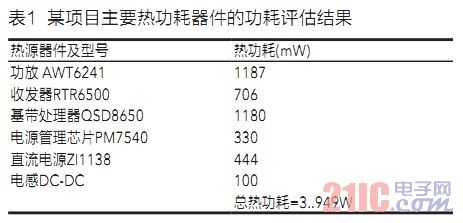
The heat source devices of the terminal platform mainly include baseband chips, radio frequency chips, power amplifiers, power management chips, etc. The power consumption of these devices can be found in the datasheet given by the manufacturer, and some can not be found, which cannot be found from the datasheet. The heat source device of the power consumption data needs to be estimated based on the test data of experience or similar projects, and the relevant data can be obtained directly from the platform provider. Table 1 shows the power consumption evaluation results of the main thermal power devices of a project.

From the data in Table 1, we can see that the power consumption of a data card is close to 4W. In order to dissipate such a large amount of heat in the U disk-sized structural components, the thermal design of the PCB can be said to have become a product. A critical design consideration for reliable work.
A thermal layout algorithm for card terminal products
The empirical value of the heat flux density of natural convection cooling is 0.8 mW/mm2, that is, when the power distributed over the area per square millimeter is 0.8 mW, a good natural convection cooling effect can be produced. The calculation of the thermal distance of the heat source device is based on this empirical value. The calculation method is as follows:
Let the length of a chip be L (mm) and the width be W (mm), and the power consumption of the device is Pd (mW).
To achieve natural convection cooling, the PCB area that the device should occupy is: ![]()
The thermal distance between the long side and the wide side of the device is equal, both of which are x (mm). The thermal distance is taken into account. The PCB area occupied by the device is:

The above calculation only considers the single-sided heat dissipation of the PCB. The actual PCB can be cooled on both sides. If the other components are not placed on the back of the heat source device, the copper skin on the back side can also play a heat dissipation role. The thermal distance at this time will be calculated above. Half of the data, namely: .
The PCB area occupied by the heat source device is calculated below.

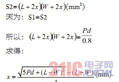
In the PCB layout, the above calculation data is often not feasible, because the PCB area is limited, if the layout according to the above data, the PCB area is not enough, so you need to compress the above data in a certain proportion, you can Dividing the above thermal distance by 2 as the thermal distance after compression, and thus calculating the compression heat distance, the PCB area occupied by the heat source device is as follows:
There is a device on the back of the heat source device, and the PCB area after compression: S1= ![]()
There is no device on the back of the heat source device, and the PCB area after compression: S2= . Table 2 calculates the layout thermal distance and layout area of ​​the heat source device of this project.

Thermal operation reliability analysis of the device
The maximum junction temperature that any heat source device can withstand is limited. This maximum junction temperature can be found in the datasheet given by the manufacturer. If the junction temperature of the actual operation of the heat source device is higher than the highest junction temperature that can be withstood, then the heat source The operation of the device will enter an unreliable state. For this case, it is necessary to consider such devices away from other heat-generating devices in the layout of the PCB. The copper area around the area is large, and the inner layer and the bottom layer directly below the location are also paved. Copper, in order to solve the problem of excessive junction temperature of such devices, so the calculation of the junction temperature of the actual operation of the heat source device is also very important in the thermal design of the PCB. In addition, it is necessary to calculate the temperature rise of the heat source device relative to the environment. Knowing the temperature rise of the heat source device relative to the environment, it is known which heat source device has the highest temperature, so that the heat distribution process will be well known.
End product thermal design algorithm and reliability application in the project
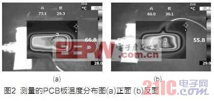
The power consumption analysis of the heat source device, the thermal distance layout area calculation of the heat source device, and the ambient temperature analysis of the heat source device can all begin the layout of the PCB. The layout of the PCB needs to follow the most basic thermal design principles, such as: hot spot dispersion; Place the device with the highest power consumption and heat generation in the best position for heat dissipation; do not place the device with higher heat on the corners and peripheral edges of the printed board; the high heat dissipation device should be able to reduce the connection between them when connecting to the substrate. The thermal resistance, etc., in addition, according to the compression heat interval calculated above, the heat source device is placed, the device is placed as little as possible within the compression heat interval of the heat source device, and the heat generating device is not disposed, and the back surface of the heat source device should be as small as possible. , can not be placed on the heating device. Figure 1 shows the final PCB layout of the project, and Figure 2 shows its temperature measurement diagram. As can be seen from the figure, the design method is practical.

"BVR", literally translated as Beyond Visual Range, is the capability of some second-generation fighters (such as F-4E) and 3rd generation, but cannot be technically due to technical reasons such as radar and other supporting software. Make BVR capabilities practical.
BVR wire Chinese name: copper core PVC insulated Soft Sheathed Wire. Wire structure: conductor + insulation.
BVR multi-core copper wire is generally used for occasions with slight movement. In addition, the BVR multi-strand line has a larger current carrying capacity than the single-strand line and the price is higher. Usually, the BVR can be used inside the cabinet, and it is not necessary to have such a large strength to facilitate wiring.
Bvr Cable,Soft Sheathed Wire,Flexible Bvr Cable,Insulation Bvr Cable
Jiangsu QiSheng Cable Co., Ltd. , https://www.shuaihe-cable.com
