A wafer is a silicon wafer used in the fabrication of a silicon semiconductor integrated circuit. Since it has a circular shape, it is called a wafer. On a silicon wafer, it can be processed into various circuit component structures to become a specific electrical function IC. product. The original material of the wafer is silicon, and the surface of the earth's crust is inexhaustible. The silica ore is refined by an electric arc furnace, chlorinated with hydrochloric acid, and distilled to produce high-purity polycrystalline silicon with a purity of up to 99.999999999%.
CPU process elements1) Wafer size
The silicon wafer size is the diameter value used by the silicon wafer during semiconductor manufacturing. The larger the silicon wafer size, the better, because each wafer can produce more chips. For example, a 0.13-micron process can also produce approximately 179 processor cores on a 200mm wafer, while a 300mm wafer can produce approximately 427 processor cores. A 300mm diameter wafer is a 200mm diameter wafer. 2.25 times, the number of processors produced is 2.385 times that of the latter, and the actual cost of 300mm wafers is not much higher than that of 200mm wafers. Therefore, this doubled productivity increase is obviously for all chip manufacturers. I like it.
However, one feature of silicon wafers limits the size of silicon wafers that manufacturers can arbitrarily increase. That is, the farther away from the center of the wafer, the more likely it is to be in the wafer production process. Therefore, the expansion from the center of the silicon wafer, the number of bad points is rising, so that we can not increase the wafer size as desired.
(2) Etch size
The etch size is a minimum size that a fabrication device can etch on a silicon wafer and is a key technical parameter for CPU core fabrication. When the manufacturing process is the same, the more transistors, the larger the processor core size, the fewer chips a silicon wafer can produce, and the cost per CPU. Conversely, if a more advanced manufacturing process means that the smaller the size that can be etched, the more chips a wafer can produce, and the lower the cost.
(3) Metal interconnect layer
In the previous section 5, "Repeat, Layering," we know that the number of internal interconnect layers for different CPUs is different. This is related to the manufacturer's design, but it can also indirectly explain the level of CPU manufacturing process. There is nothing to say about this design, Intel has fallen behind in this regard, when they use 6-layer technology on the 0.13 micron process, other vendors have used 7-layer technology; and when Intel is ready to use 7-layer, IBM Eight layers of technology have already begun; AMD has used 9-layer technology when Intel introduced seven layers of copper connections with Lowk insulation in Prescott. More interconnect layers provide greater flexibility in the production of hundreds of millions of transistor CPUs such as Prescott.
We know that as transistor sizes continue to decrease and more transistors are integrated on the processor, the metal lines connecting these transistors are even more important. In particular, the capacity of metal lines directly affects the speed of information transfer. On the 90nm process, Intel introduced a new insulating carbon-containing silica to replace the fluorinated silicate glass, which also indicates that this can increase internal interconnect efficiency by 18%.

(1) Silicon purification
The material for producing chips such as CPU is semiconductor. The main material at this stage is silicon Si, which is a non-metallic element. From a chemical point of view, it is at the junction of the metal element region and the non-metal element region in the periodic table. It has the properties of a semiconductor and is suitable for manufacturing various tiny transistors. It is one of the materials most suitable for the manufacture of modern large-scale integrated circuits.
During the silicon purification process, the raw silicon is melted and placed in a huge quartz furnace. At this time, a seed crystal is placed in the furnace so that the silicon crystal grows around the seed crystal until a nearly perfect single crystal silicon is formed. Previous silicon ingots were mostly 200 mm in diameter, and CPU manufacturers are increasing the production of 300 mm wafers.
(2) Cutting the wafer
The ingot is made and shaped into a perfect cylinder, which is then cut into sheets called wafers. Wafers are really used in the manufacture of CPUs. The so-called "cut wafer" is to use a machine to cut a predetermined silicon wafer from a single crystal silicon rod and divide it into small areas, each of which will become a CPU core (Die ). In general, the thinner the wafer is cut, the more CPU products can be manufactured with the same amount of silicon material.
(3) Photolithography
A photoresist (photoresist) is applied on the silicon oxide layer obtained by the heat treatment, and the ultraviolet ray is irradiated to the silicon substrate by a template printed with a complicated circuit structure pattern of the CPU, and the photoresist is dissolved by the ultraviolet ray. In order to avoid interference with light that is not required to be exposed, a mask must be made to cover these areas. This is a fairly complicated process, and the complexity of each mask is described by 10 GB of data.
(4) Etching
This is an important operation in the CPU production process and a major technology in the CPU industry. Etching technology pushes the application of light to the limit. The etching uses a very short wavelength of ultraviolet light and is matched with a large lens. Short-wavelength light will be transmitted through the apertures of these quartz masks onto the photoresist film to expose them. Next, the illumination is stopped and the mask is removed, and the exposed photoresist film is washed away with a specific chemical solution, and a layer of silicon that is in close contact with the resist film underneath.
The exposed silicon will then be bombarded with atoms, causing the exposed silicon substrate to be partially doped, thereby changing the conductive state of these regions to create a N or P well. Combined with the substrate fabricated above, the CPU gate is completed. It is.
(5) repetition, layering
In order to process a new layer of circuit, silicon oxide is grown again, then a layer of polysilicon is deposited, a photoresist is applied, and photolithography and etching processes are repeated to obtain a trench structure containing polysilicon and silicon oxide. Repeat multiple times to form a 3D structure, which is the core of the final CPU. Metal is used as a conductor in the middle of each layer. Intel's Pentium 4 processor has 7 layers, while AMD's Athlon64 has 9 layers. The number of layers depends on the layout of the CPU at design time and the amount of current passed.
(6) package
The CPU at this time is a piece of wafer, which is not directly usable by the user. It must be enclosed in a ceramic or plastic package so that it can be easily mounted on a circuit board. The package structure is different, but the more advanced the CPU package is more complicated, the new package can often bring about the improvement of the chip's electrical performance and stability, and can indirectly provide a solid and reliable basis for the improvement of the main frequency.
(7) Multiple tests
Testing is an important part of CPU manufacturing, and it is also a necessary test before the CPU leaves the factory. This step will test the electrical performance of the wafer to check for any errors and where (if possible) these errors occur. Next, each CPU core on the wafer will be tested separately.
Since SRAM (static random access memory, the basic composition of the cache in the CPU) has a complicated structure and high density, the cache is a part of the CPU that is prone to problems, and the test of the cache is also an important part of the CPU test.
Each CPU will be fully tested to verify its full functionality. Some CPUs can operate at higher frequencies, so they are labeled at a higher frequency; while some CPUs operate at lower frequencies for a variety of reasons, they are labeled at a lower frequency. Finally, individual CPUs may have some functional flaws. If the problem is in the cache, the manufacturer can still block its partial cache, which means that the CPU can still be sold, but it may be a low-end product such as Celeron. .
Before the CPU is placed in the box, the last test is usually done to ensure that the previous work is accurate. They are packaged in different packages and sold around the world, depending on the highest operating frequency and cache previously determined.
How does the wafer become cpuAs early as 2010, the European Union sponsored a project initiated by the University of Heisenberg, Germany, called BrainScaleS (Brain-inspiredmultiscalecomputationinneuromorphichybridsystems), which is similar to the recently fired IBMTureNorth processor, which simulates the physical structure of the brain. However, they simulate the brain structure of the mouse. The specific steps are to freeze the brain of the mouse with liquid nitrogen, then use a machine to rub it off layer by layer. Take a picture every time the layer is ground, and then study according to all the photos. The brain structure of the mouse (yes, the same method used for copying boards for cottage phones).

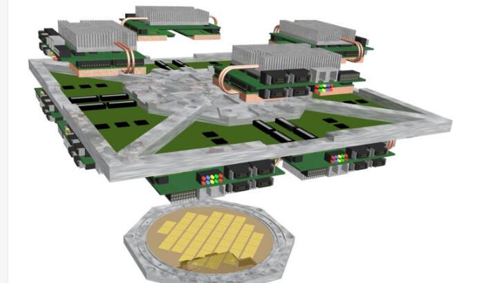
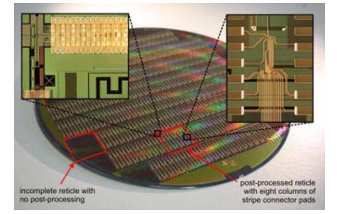
Then according to this 180nm CMOS process, the mouse brain structure was reproduced in a whole 8-inch wafer, with 200,000 neurons and 50 million synapses. Because the brain is a 3D-like network structure, the actual CPU is flattened onto a 2D plane, so there is a single area on the wafer, and a specially developed structure is used between the different areas. Connected.

As for why such an "antique" process is used, the reason is that this is a digital-analog hybrid chip. We know that analog circuits cannot use semiconductor processes with too small line width due to their own characteristics (low noise and high driving capability, etc.) Either you can't reach the design index, or you just burn it out, and digital circuits don't need to think about it. So today, the CPU process has progressed to 14nm, the mainstream process used in analog circuits is still 130-180nm.

The actual system has been launched in 2013, but the effect seems to be not as good as expected, this project has stopped last year.
The telecom parts are metal or plastic equipment which is used for the purposes of telecommunication, like as telecom equipments and IT hardware: LSA Module, Krone Module, Disconnection Module, Distribution box, Label holder, Test plug, Wiring block, Rack screws
When you buy from Uonicore Electronics, you get quality telecoms equipment, good lead times, original parts and continued support for legacy equipment. In addition, you can support your environmental credentials with our recycling options and use of refurbished equipment.
Telecom Parts,telecommunication parts,telecom components,Server Rack Mount Screws
NINGBO UONICORE ELECTRONICS CO., LTD , https://www.uniconmelectronics.com
