Serial communication refers to the sequential transmission of data bit by bit using a transmission line. The utility model has the advantages that the communication line is simple, the communication can be realized by using a simple cable, the cost is reduced, and the application is suitable for long-distance communication, but the transmission speed is slow.
Asynchronous communication uses one character as the transmission unit. The time interval between two characters in communication is not fixed, but the time interval between two adjacent bits in the same character is fixed.
The data transfer rate is expressed in baud rate, which is the number of binary bits transmitted per second. For example, if the data transfer rate is 120 characters/second and each character is 10 bits (1 start bit, 7 data bits, 1 check bit, 1 end bit), the baud rate of the transfer is 10 & TImes. ;120=1200 characters/second=1200 baud.
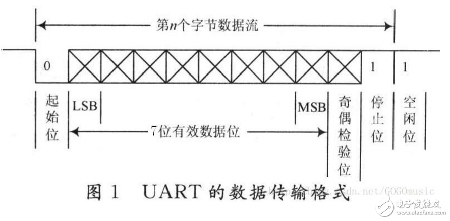
The data communication format is as follows:

Start bit: A logic "0" signal is sent first to indicate the beginning of the transmitted character.
Data bits: can be 5~8-bit logic "0" or "1". Such as ASCII code (7 bits), extended BCD code (8 bits).
Check Digit: When the data bit is added to this bit, the number of bits of "1" should be even (even parity) or odd (odd parity).
Stop bit: It is the end of a character data. It can be a high level of 1 bit, 1.5 bits, or 2 bits.
Idle bit: In the logic "1" state, there is no data transmission on the current line.
Asynchronous communication is transmitted by characters. After receiving the start signal, the receiving device can receive correctly by keeping the synchronization with the transmitting device within one character transmission time. The arrival of the start bit of the next character causes the synchronization to be recalibrated (by detecting the start bit to achieve self-synchronization of the transmit and receive clocks)
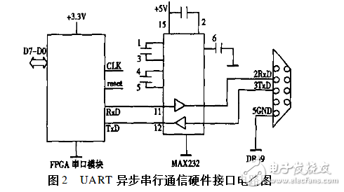
Principle design of hardware interface circuit for serial communicationIn serial communication, the standard of the RS-232-C interface is commonly used. The connection mode of the RS-232-C interface signal pin specifies a 25-pin D-type connector (DB225). In practice, a 9-pin D-type connector (DB29) is used. This solution uses a DB29 connection. Device

The hardware interface circuit diagram of the asynchronous serial communication of this scheme is shown in Figure 2. It consists of three parts: FPGA serial port module, MAX232 and DB29. MAXIM's MAX232 is designed to meet the EIA/TEA2232E standard. It features low power consumption, high baud rate, and low price. The operating power supply is +5V, and the external capacitor is only 0.1uF or 1Uf. It is a dual-group RS2232. transceiver. The MAX232 has two transmitters. If only one of the transmitters is used, the input and output of the other transmitter can be left floating. This scheme implements the asynchronous communication circuit as a whole. The data is input from the RxD terminal of DB29. The level conversion by MAX232 is entered by the RxD terminal of the FPGA serial port module, and serial-to-parallel conversion is performed to enter the FPGA via the 8-bit data bus (D72D0). Other modules or other processing chips. After the data is processed, it enters the FPGA serial port module through the 8-bit data bus. After the parallel-to-serial conversion, the 12-pin of the MAX232 is output by the TxD terminal, and is outputted by the TxD terminal of the DB29 after the MAX232 type is level-converted.
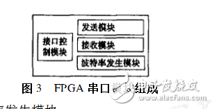
FPGA serial module designThe FPGA serial port module is the key to this design, the internal logic structure and the functions of each component. As shown in FIG. 3, it mainly consists of a baud rate generation module, a transmission module, and a receiving module. The function description of each component designed with Verilog is shown in Figure 3.

The designed UART is received and transmitted at the same baud rate, and the baud rate can be set via the bus interface of the interface module. Each data width of the UART transceiver is 16 times of the clock period output by the baud rate generator. That is, assuming that the current transmission and reception is performed at 9600 b/s, the output clock frequency of the baud rate generator should be 9600&TImes; 16 Hz. Assuming an external clock of 1.6MHz, it is easy to write different values ​​to the baud rate generator holding registers via the bus, and then generate the various baud rates required by the counter, ie the divider. The calculation formula is: 1600000 / (16 & TImes; the desired baud rate) -1, if you want to output the baud rate of 10000Hz, you can get the value written from the bus is 1600000 / (16 & TImes; 10000) -1 = 9 ( 09H).
Sending moduleAccording to the description of the UART protocol, the transmission data is controlled by the interface module, the interface module gives the wrn signal, the transmitter latches the parallel data according to the signal, and transmits the parallel data through the transmission holding register and the transmission shift register. The state of the control is controlled by the counter no-bs-sent, that is, the data is transmitted. When the count value is 1, the data is transferred from the transmission holding register to the transmission shift register. When the count value is 2, the transmission start bit (1b low level) is transmitted. The count value is 3~10, the 8-bit data is sent, the counter is 11, the check digit is sent, the count value is 12, the 1-bit stop bit is sent, and the counter is subsequently cleared. The transmit clock is generated based on the baud rate of the data transfer, 16 times the clock generated by the baud rate generator.
In Xilinx's ISE7.1.02i integrated environment, code is written in Verilog, Synplifypro8.1 is used for logic synthesis, and Modelsim6.0d is simulated. The result is shown in Figure 4.

The receiving logic first checks the start bit by detecting the falling edge of the input data, then generates a receive clock, samples the serial input data with the receive clock, performs a shift operation in the buffer, and generates a check bit at the 9th bit. Check whether the check digit is correct, compare whether the stop bit is high at the 10th bit, and generate an error indication signal if the check digit is wrong or the stop bit is wrong. The receive clock is generated based on the baud rate of the data transfer, 16 times the clock generated by the baud rate generator.
The timing simulation of the receiving module is done using Modelsim6.0. The result is shown in Figure 5. The receiving clock is the same as the transmitting clock, receives one frame of serial data, is converted into parallel output by the receiving module, and checks the parity bit and the stop bit to generate framing-error and parity-error signal outputs.

The interface control module is connected to control the transmit, receive, and baud rate generation modules, and is connected to the external parallel bus to receive control signals (nrst, nwrn, nbdn, nrdn) from the external (CPU or microcontroller) to control the transmission and reception of the UART. And the generation of the internal clock. When nwrn is valid and the internal signal tbre='0' (transmission buffer register empty), the parallel data input from the data bus is transmitted to the transmission module data line din(7:0), and the transmission data function is executed. When nrdn is valid and the internal signals data-ready, parity-error, and framing-error are valid, the received data is allowed to be read from the receiving module. The baud rate generator and the parallel data input port of the transmit module share a single data bus.
Comprehensive performance analysisUsing Xilinx's Spatan IIxc2s100 FPGA chip, Synplifypro8.1 is used for logic synthesis of the entire FPGA design. In fact, the total FPGA resources occupied are only 56 lookup tables (LUTs), which occupies very little resources and can be easily integrated into other FPGA designs. Medium; the maximum clock speed can reach 121.8MHz, it can be seen that this design can fully meet any standard baud rate series
Hardware circuit implementation and software implementationIn validating this UARTFPGA design, PADS was used to design the schematic and PCB diagrams, and finally downloaded and debugged successfully on the hardware. When verifying UART communication, the PC serial communication program of this design is implemented by the Ac2tiveX control method.
The UART communication function is realized by FPGA, which can realize the receiving and transmitting of data, and can judge its check bit and stop bit when receiving data, and form a complete one-frame data format when transmitting data. The clock for receiving and transmitting data is generated by an internal baud rate generator, and the external clock is divided according to a preset frequency division coefficient to generate a required receiving or transmitting clock. By embedding the UART FPGA design as a functional block into an FPGA-implemented data acquisition and processing system, asynchronous serial communication with a remote PC can be successfully implemented. The experiment proves that the UART design occupies less resources, works stably and reliably, and can be used in low-end asynchronous communication.
Distribution Box
Distribution Box,Distribution Boxes TUV,CE Distribution Boxes,Distribution Boxes
Wenzhou Korlen Electric Appliances Co., Ltd. , https://www.zjmotorstarter.com
