The attitude and attitude signal simulator is designed to provide a manually adjustable and controlled signal source for the instrumentation or laboratory research to be tested. It can generate aeronautical attitude signals of various frequencies and arbitrary waveforms defined by the user, etc. Aircraft performance is tested. The development of the traditional attitude and attitude signal simulation system is based on VXI, PCI and other buses. Most of them use hardware circuit design and implementation. The PC is used for analysis and processing. The function is relatively perfect, but the structure of the circuit is complex and the volume is too large. It is huge, not suitable for use in the field, and the traditional simulator is limited in scope, which causes a lot of waste in terms of cost. Therefore, it is very necessary to develop a new type of programmable universal simulator. This paper is designed to be a portable attitude and attitude signal simulator, which is not only small in size but also easy to carry, and the processor uses a DSP with high-speed data computing capability. Pre-processing, transmission, display and storage of the shaft angle signal output from the resolver. The system can be widely used in military equipment such as aviation, aerospace, radar and artillery control, and can also be used in civil equipment such as CNC machine tools and robots, and has broad application prospects.
Power supply design
Because the DSP chip uses two different voltages, the core 1.8 V voltage and the IO port 3.3 V voltage, the dual power supply is generally used for the DSP system power supply. In this design scheme, TI's power supply chip TPS767 (DSP) is specially used for the DSP. 1.2375) D301 provides power supply. This chip is a linear DC/DC converter chip. It can supply 3 V DC power supply to TPS767 ($1.2375) D301 to generate 3.3 V and 1.8 V voltages for F2812, and directly supply power to DSP. In addition, the maximum output current of this power chip can reach 1 A, which can supply power to the DSP chip and a small number of peripheral circuits at the same time.
Clock and reset circuit
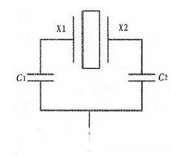
The clock of the DSP2812 chip has two kinds of pin connection. One is to use the crystal circuit provided in the internal circuit to connect a crystal between its X1/XCLKIN and X2 pins to start the internal oscillator; the other is to directly The external clock source is directly input to the X1/XCLKIN pin, and the X2 pin is left floating. The first method is used in this design, as shown in Figure 3.

The DSP2812 chip has a phase-locked loop clock module (PLL) that can be multiplied by the input clock. Therefore, a 30 MHz external crystal oscillator can be used to achieve the system's 150 MHz requirement after phase-locked loop multiplication. Since the power module TPS767 ($1.2375) D301 chip can generate a reset signal itself, and this reset signal can be directly used by the DSP chip, there is no special reset chip in this design.
Switch chip working principle and its interface design with DSP
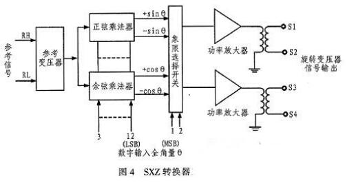
The 12SXZ conversion chip consists of the following parts: reference transformer, quadrant selection switch, sine and cosine multiplier, power amplifier, output transformer and other five parts. After the digital full-angle and reference signal input is passed through the sine and cosine multipliers, it is converted into a sine and cosine signal representing the angle, and then amplified by the power amplifier, having a load capacity of 1.3VA, and then isolated and boosted by the output transformer. It becomes a three-wire, four-wire analog signal output in the form of a self-aligning machine/resolver.
The left side of the equation is the output voltage, θ is the input digital angle, K is the proportional coefficient, and URH-RL is the reference voltage. The working principle block diagram of the converter is shown in Figure 4.

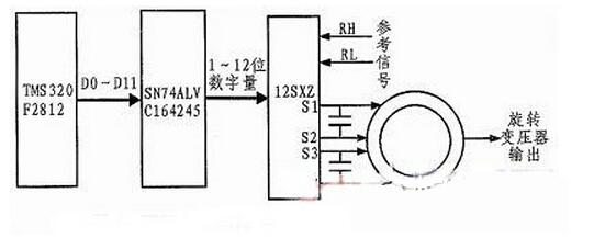
The core of the simulator is DSP 2812. It can generate the required attitude and attitude signals through software control, and the system has self-checking function. In the system design, the DSP controls the I/O port to directly operate the 12SXZ to generate analog signals. We know that DSP has two kinds of voltages. The voltage of I/O port is 3.3 V. The conversion chip we use is TTL level 5 V. Considering the driving ability of DSP to generate signals, we need level conversion first, and DSP. The 3.3 V level of the port output is converted to 5 V. The level shifting chip used is the SN74ALVC164245 ($0.8750), which is a 16-way bidirectional level-shifting chip controlled by the pin DIR. The conversion chip SXZ is a 12-bit number converter, and is connected with 12 channels of the level conversion chip by the data ports D0 to D11 of the DSP, and the converted 12-bit level is connected to the 12-bit digital input terminal of the SXZ. The interface circuit between DSP and 12SXZ converter is shown in Figure 5.

This paper introduces the hardware design circuit of the attitude and attitude signal simulator based on DSP technology. This method overcomes the shortcomings of traditional analog technology, such as complex structure, low precision and poor reliability. Through the software programming, the heading attitude signal can be realized. Through the development, debugging and application of the simulator, the simulator has the advantages of low power consumption, low volume and small volume, which is convenient for on-site debugging, can be used in various environments, and can eliminate the aircraft. Significant improvements will be made in terms of failure and maintenance of aircraft safety and improved flight quality.
The core control chip chosen for the design is the TMS320F2812 ($18.5250), but basic peripheral circuitry must be provided to function as a core control circuit. A typical DSP minimum system should include a DSP chip, a power supply circuit that provides the appropriate power for the DSP chip, a reset circuit that triggers the DSP initialization, a clock circuit, and a JTAG interface circuit for in-circuit emulation and download. In addition, due to the need to communicate with the host computer, complete the transmission of data and control signals, a serial communication circuit is added on this basis. The basic system block diagram of DSP is shown in Figure 2. The external RAM is used to place a large amount of signal data, and the extended FLASH ($44.9500) is used to store the control program.
Fast thyristors (Inverter Thyristor)are used for higher frequency rectification. Inverter and inverter circuit appliances.
Rectifiers have many uses, but are often found serving as components of DC power supplies and high-voltage direct current power transmission systems. Rectification may serve in roles other than to generate direct current for use as a source of power. As noted, detectors of radio signals serve as rectifiers. In gas heating systems flame rectification is used to detect presence of a flame.
Inverter Thyristor,Power Inverter Thyristor,Frequency Inverter Thyristor,Electronic Component Inverter Thyristor,Bi-directional Controlled Thyristors (BCT)
YANGZHOU POSITIONING TECH CO., LTD. , https://www.cnpositioning.com
