In the past few years, Apple's chip design team has been at the forefront of architecture design and manufacturing processes. Apple A12 is another leap of the company across generations, because it claims to be the first commercial 7nm chip. After TechInsights publicly shared the picture of Apple's A12 chip, anandtech website subsequently released the first analysis and commentary on the photo of the die.
When talking about process nodes, generally speaking, the smaller the number, the smaller the transistor. Although the connection between the name of the node and the actual physical size has long lost its meaning recently, it still represents a leap in density. Therefore, suppliers can package more transistors in the same chip space.
Thanks to TechInsights for publicly sharing the picture of Apple’s A12 chip, we subsequently released the first analysis comment of the die photo:
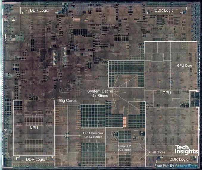
Photo of Apple's A12 chip die (Source: TechInsights)
In this article, I reviewed the A12 chip again, and I wrote down my own definition of tags and explanations for the photos of the die. The new A12 chip mainly follows Apple's SoC layout structure (rotated by 90 degrees compared to most die in the past).
On the right, we see the GPU complex, with four GPU cores and shared logic in the middle. The CPU complex is located at the bottom. There are two Vortex large CPU cores on the left side of the middle, separated by a large L2 cache, next to 4 small CPU cores and their respective L2 caches.
The four large SRAM blocks in the middle are part of the system cache, which is the SoC-wide cache layer, located between the memory controller and the internal system interconnection and the block memory subsystem. Apple uses this block as an energy-saving function: because DRAM memory transactions are very expensive in terms of energy use, caching on the chip will save a lot of power, and due to the locality of data, performance may be improved, which will bring Comes with additional benefits.
So far, the system cache of the Apple A12 has seen the biggest change since the launch of the Apple A7. The huge change in the layout also shows the huge change in the function of the block, because now we clearly see that the block is divided into 4 obvious parts. In previous Apple SoCs, such as A11 and A10, the system cache looks more like a logical block, and it seems to be two parts. The doubling of part of the block may indicate that the memory performance of this block has changed a lot. In the following article, I will conduct a more detailed analysis.
The last important introduction about A12 is a major improvement of the neural network accelerator IP. Apple claims to have switched from the dual-core design of the A11 to the new 8-core design. In the speech, it is very important that Apple has never mentioned that this is an internal design, and marketing materials are always eager to introduce other IP blocks of SoC.
It is rumored that the design last year was CEVA IP, but we have never been fully confirmed because Apple does not want it to be known by people. A12 is an 8-core design with a performance increase of 4 times, but the actual performance increase is close to 8 times, from A11's 600GigaOP to A12's 5TeraOP. In the die photo, we see 8 MAC engines surrounding a large central cache, and there may be a shared logic part at the top, responsible for fixed-function and fully-connected layer processing.
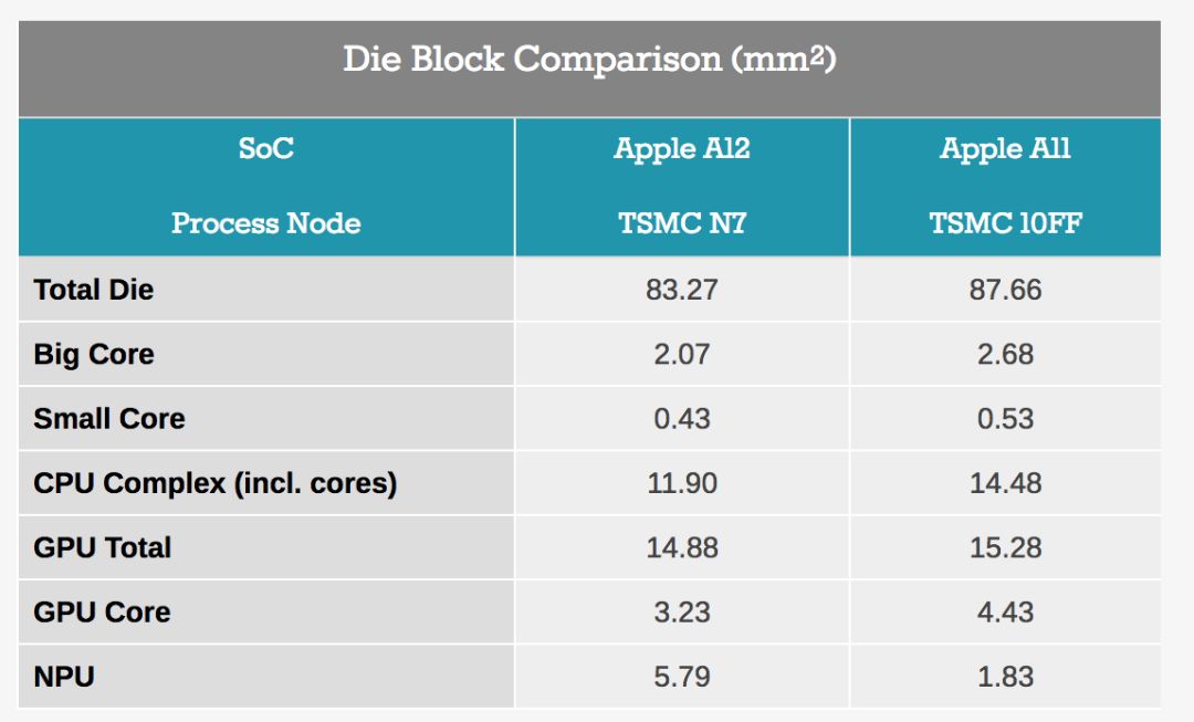
Looking at the changes in different block sizes from A11 to A12, we see the advantages of TSMC’s new 7nm process node. It is worth noting that almost all IP blocks have undergone changes, so the comparison of A11 vs A12 to determine how much the density of the new process node has increased is not an effective method. Nevertheless, we took a single GPU core as a possible candidate (because the structure we saw was basically the same), and observed that compared with A11, the size of A12 was reduced by 37%. It is obvious that the new node allows Apple to add an additional GPU core, but in absolute terms, the GPU in the A12 is still smaller.
Larger CPU and large-scale cache hierarchy

Source: TechInsights' Apple A12 die photos, ChipRebel's Apple A11 die photos
Next is the CPU complex, especially the new large CPU core. What we are seeing now may be the biggest change in the CPU layout of Apple's several generations of chips. In particular, we see that the L1 data cache in the new Vortex CPU has doubled, from 64KB to 128KB. On the front end, we also saw double SRAM blocks, which I attributed to the L1 instruction cache, and I now believe it must have doubled to 128KB. What’s interesting is that even today, a few years later, we still haven’t really figured out what A10 introduced in the front-end block: here, we see a new very large cache block, the specific function of which is not yet clear. .
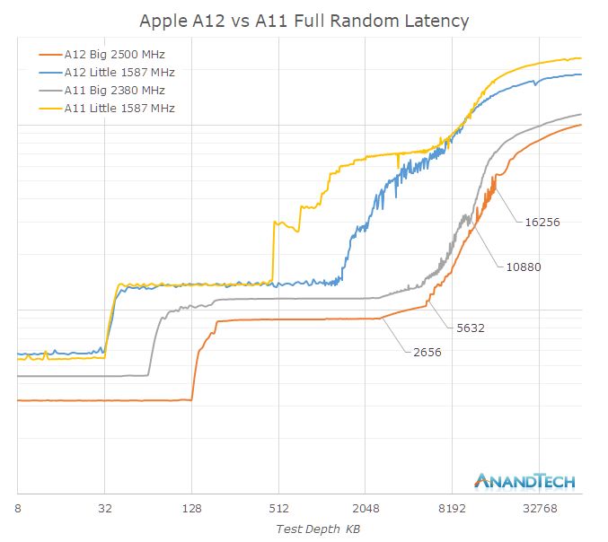
A big question over the years has been what Apple’s cache hierarchy looks like. Looking at the memory latency behavior under different test depths, we can see different jumps under different test depths. I did not label the delay values ​​because we will see them again in the non-logarithmic version of this graph later.
In terms of the big core, we clearly see L1$ jump from 64KB to 128KB, I think there is no doubt about the growth here. However, entering the L2 cache, we saw some strange characteristics in terms of latency. Obviously, in the range of 3MB, the delay increases until about 6MB. It is worth noting that only when accessing in a completely random mode, the delay will slowly increase around 3MB. In a smaller access window, the delay is always flat until 6MB.
We no longer consider this issue for the time being, and instead enter the 6MB or more area of ​​the system cache service. It is difficult to figure out at first because the overall low latency will cause offset, but overall, before we reach the DRAM latency, the latency curve will further increase by about 4MB. This is consistent with what we actually see on the die: the new system cache not only doubles the divided part of the block, but also doubles the capacity from 4MB to 8MB.
When we analyze the small core next, things get a little complicated. At first glance, you would believe that the small core L2 of the A11 is limited to 512KB, while the A12 is up to 1.5MB. However, I think we are being deceived by the power management strategy of the cache. Looking at the A11 Mistral core latency, we can see a clear jump at 768KB and 1MB. A12 core can also see a similar jump at 2MB.
At this point, we'd better go back to the bare picture and do some pixel calculations to get the following table:
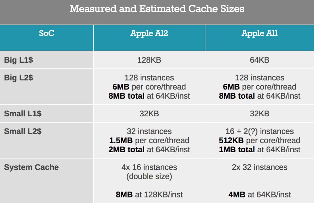
The big core L2 does not have any structural changes between A11 and A12. Both have 128 SRAM macros instances, which are divided into two blocks. The problem here is still that if L2 is indeed only 6MB, then this means 48KB per SRAM block.
When looking at the small cores, we see that they use the same SRAM macros. The small core L2 of A12 has increased from 16 instances to 32, which means there must be a doubling here. However, as we have seen, the measured delay depth of L2 has increased by at least three times, and other things must be happening. The data we measured by no means represents the content of the hardware. In fact, we can confirm this by running a delay test in a more specific way, which makes the power management think it is just a small workload. In A12, Tempest core seems to be only 512KB available.
The conclusion is that Apple uses partial cache power shutdown on the interval scale of each bank. On A12, the L2 bank of each small core is 512KB, while on A11 it is 256KB. Moreover, this makes me firmly believe that there is 2MB on A12 and 1MB on A11, but the test may not meet the policy requirements of accessing the full cache.
In turn, because this will confirm that each SRAM instance is 64KB, we can go back and make some assumptions about the big core L2. Please look again, you will think it stays at 6MB, but look carefully, especially A12, the characteristics have changed at 8MB. Similarly, the kernel may have 8MB of physical cache, and once we get close to the full cache, the access behavior will change significantly.
The point here is that Apple's cache is very large, and A12 has further expanded in this regard, doubling the size of the system cache. In practice, we have about 16MB of available cache hierarchy on large CPU cores-this huge amount will only dwarf the memory and cache subsystems of SoC competitors.
Attacking GPU
In terms of GPU, we have great expectations for A12, not only in terms of performance, but also in terms of architecture. Last year, Imagination issued a press release claiming that Apple has notified them that the company plans to no longer use its IP in new products within 15 to 24 months. This eventually caused the stock price to plummet, and the company was subsequently sold to an equity company.
Therefore, even though Apple claims that the A11 GPU is an internal design, it still looks like an Imagination derivative design, because its block design is very similar to the previous Rogue-the biggest difference is that the so-called core is now larger than the previous two. A larger structure at the core. In fact, it is still a TBDR (tile-based deferred rendering), IMG has many patents, but an important fact is that Apple still very public and support PVRTC (PowerVR texture compression, a proprietary format), which means The GPU may still be associated with IMG’s IP. Here, we may still think that it is an architectural permission design, rather than what we usually call a "clean" design.
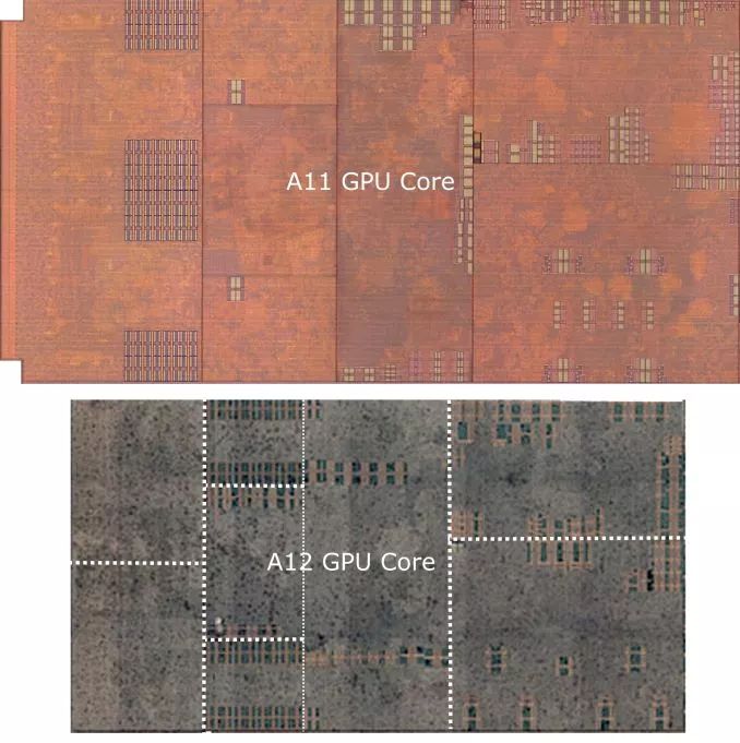
Source: TechInsights' Apple A12 die photos, ChipRebel's Apple A11 die photos
Let's look at the A12 GPU again. The model is named G11P. We see some very obvious similarities with last year's A11 GPU. The various functional blocks seem to be located in the same location to a large extent and are structured in a similar way.
I think the biggest advancement of Apple's A12 GPU is to support memory compression. I was very surprised to hear this news at the press conference, because it also means two things: the previous Apple SoC and GPU obviously did not have memory compression, and now this alone is enough to significantly improve the performance of the new GPU.
The so-called memory compression, especially refers to the transparent frame buffer compression from the GPU to the main memory. In the desktop field, vendors like Nvidia and AMD have had this feature for many years, and it can improve GPU performance even if the memory bandwidth has not increased. Smartphone GPUs also require memory compression, not only because of the limited bandwidth on the mobile SoC, but most importantly because of the reduced power consumption associated with high bandwidth requirements. ARM's AFBC has always been the most publicly discussed mechanism in the mobile field, but other vendors such as Qualcomm and even Imagination have their own implementation mechanisms.
Apple seems to have introduced this feature through the A12 very late, but it also means that the A12 will benefit from a huge intergenerational improvement in efficiency and performance. Considering that Apple has announced that it will substantially add new GPUs, this move is of great significance.
A12 Vortex CPU Tour
When talking about the Vortex microarchitecture, the first thing we need to discuss is the frequency we see on Apple's new SoC. In the past few generations, Apple has been steadily increasing the frequency of its big core, while also increasing the IPC of the micro-architecture. I conducted a quick test on the frequency characteristics of A12 and A11, and got the following table:

The maximum frequency of the A11 and A12 is actually a single-threaded boost clock-the Monsoon core of the A11 is 2380MHz, and the new Vortex core of the A12 is 2500MHz. In the application of ST, this is only a 5% frequency increase. When the second large thread is added, the A11 and A12 clocks are reduced to 2325MHz and 2380MHz, respectively. When we were running threads on a small core at the same time, the situation between the two SoCs diverged: A11 further dropped to 2083MHz, while A12 continued to stay at 2380MHz until it reached the thermal limit and eventually stopped working.
In terms of small cores, compared to the previous Mistral, the new Tempest core is actually more conservative. When the system only runs a small core on A11, the maximum frequency is increased to 1694MHz. This feature is now gone on the A12, and the maximum frequency is 1587MHz. When the 4 small cores are fully loaded, the frequency is further reduced to 1538MHz.
Greatly improved memory latency

As mentioned earlier, it is clear that Apple has invested a lot of work in the A12's cache hierarchy and memory subsystem. Returning to the linear delay graph, we can see that the completely random delay for the large core and the small core has the following characteristics:
Compared with the Monsoon core, the frequency of the Vortex core has increased by only 5%, but the absolute L2 memory latency has dropped from 11.5ns to 8.8ns, an increase of 29%. This means that the L2 cache of the new Vortex core can now complete operations in fewer cycles. In Tempest, the L2 cycle delay seems to remain the same, but there have been major changes in L2 partitioning and power management, allowing access to larger physical L2 chunks.
I only conducted in-depth tests in the range of less than 64MB. Obviously, in the test data set, the delay curve has not flattened out, but it can be seen that the delay of DRAM has improved. When the small core is active, the maximum value of the DVFS frequency of the memory controller will increase, which can explain why the DRAM access of the Tempest core has a large difference-when there are large threads running on the large core, their performance will be better.
The system cache of A12 has undergone tremendous changes in its characteristics. Although the bandwidth of this part of the cache hierarchy is reduced compared to A11, the latency has been greatly improved. An important impact here can be attributed to the L2 prefetcher. I have also seen the possibility of a prefetcher on the system cache side: both the latency performance and the number of stream prefetchers have been improved.
Instruction throughput and latency
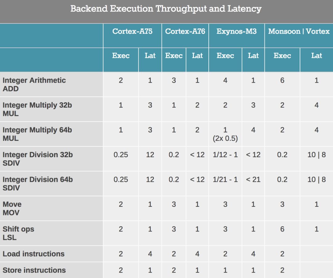

In order to compare the back-end features of Vortex, we tested the instruction throughput. The back-end performance is determined by the number of execution units, and the delay is determined by the quality of the design.
The Vortex core looks very similar to the previous Monsoon (A11), except that we seem to have found a new division unit because the execution delay is reduced by 2 cycles in both integer and FP. In terms of FP, the division throughput has doubled.
From the central and back-end point of view, Monsoon (A11) is an important micro-architecture update. It is here that Apple changed the micro-architecture of Hurricane (A10) from 6-wide decoding to 7-wide decoding. The most important change in the backend is the addition of two integer ALU units, from 4 units to 6.
Monsoon (A11) and Vortex (A12) are extremely wide machines-with 6 integer execution pipelines, including two complex units, two load units and storage units, two branch ports, and three FP/vector pipelines , Which gives an estimated 13 execution ports, far exceeding ARM’s upcoming Cortex A76, and wider than Samsung’s M3. In fact, assuming we don’t see atypical shared ports, Apple’s microarchitecture seems to be much wider than anything else, including desktop CPUs.
SPEC2006 performance: reach the desktop level
We have been experimenting with SPEC on iOS devices for some time-due to various reasons, we have been unable to continue experimenting with SPEC in the past few years. I know that many people hope that we can start again where we left off, and I am happy to tell you that I spent some time getting SPEC2006 back into use.
SPEC2006 is an important industry standard inspection benchmark. The difference from other workloads is that it handles larger and more complex data sets. Although GeekBench 4 has become a popular industry benchmark-I appreciate the effort to achieve a fully cross-platform benchmark-but we must consider that the program size and data size of the workload is still relatively important. Therefore, SPEC2006 is better as a benchmark. It fully demonstrates more details of a given micro-architecture, especially in terms of memory subsystem performance.
The following SPEC data are estimates because they have not been submitted and formally verified by SPEC. The compilation settings of the benchmark library are as follows:
Android: Toolchain: NDK r16 LLVM compiler; Flags: -Ofast, -mcpu=cortex-A53
iOS: Toolchain: Xcode 10; Flags: -Ofast
On iOS, 429.mcf is a problem because the kernel memory allocator usually refuses to allocate the single large 1.8GB chunks that the program needs (even for the new 4GB iPhone). I modified the benchmark to use only half of the arc, thereby reducing the memory footprint to about 1GB. I measured the reduction in running time on several platforms and applied a similar scale factor to the iOS scoring. I estimated the accuracy of the scoring to be +-5%. The remaining workloads are manually verified and verified whether they are executed correctly.
The performance measurement is run in an artificial environment (ie: use a desktop fan to cool the phone), and we guarantee that within the 1-2 hours required to complete a full set of operations, heat will not be a problem.
In terms of data display, I refer to articles from earlier this year, such as our evaluation of Snapdragon 845 and Exynos 9810 in the Galaxy S9 review.
When measuring performance and efficiency, it is important to consider three indicators: Obviously, the performance and running time of the benchmark test are expressed on the right axis and grow from the right. The larger the data, the better the performance of the SoC/CPU. The label represents the SPECspeed score.
On the left axis, the bar graph represents the energy usage for a given workload. The longer the bar, the more energy the platform uses. The shorter the bar, the more energy-efficient the platform means, the less energy it uses. The label represents average power (expressed in watts), which is an important secondary indicator considered in thermally constrained devices, and total energy (expressed in joules), which is the main efficiency indicator.
The data is arranged in the order in the legend, and different colors represent different SoC vendors and different generations. I listed the data for Apple A12, A11, Exynos 9810 (2.7 and 2.3GHz), Exynos 8895, Snapdragon 845 and Snapdragon 835. This gives us an overview of all relevant CPU microarchitectures over the past two years.
We start with the SPECint2006 workload:

Under most workloads, the clock frequency of the A12 is 5% higher than that of the A11, but we must remember that we cannot really lock the frequency on the iOS device, so this is just an assumption of the runtime clock during the benchmark test. In SPECint 2006, A12 performed 24% better than A11 on average.
The smallest increase is seen in 456.hmmer and 464.h264ref-they are the two most executed bottlenecks in the entire set of tests. Since A12 does not seem to have changed much in this regard, the small increase is mainly due to higher frequencies and improvements in the cache hierarchy.
445. The improvement of gobmk is very large, reaching 27%-the workload characteristics here are bottlenecks in storage address events and branch mispredictions. I did measure that A12 has some major changes in the way it handles the storage of cache lines, because the branch prediction accuracy has not changed significantly.
Part of 403.gcc, 429.mcf, 471.omnetpp, 473.Astar and 483.xalancbmk are very sensitive to the memory subsystem. At this time, the performance of A12 has increased from 30% to 42%, which is shocking. Obviously, the new cache hierarchy and memory subsystem have achieved great results in this regard, because Apple has achieved one of the most important performance leaps in recent generations of chips.
When measuring power efficiency, we found that overall A12 has increased by 12%, but we must remember that we are talking about a 12% reduction in energy consumption at maximum performance. The A12 showed a 24% increase in performance, and the performance/power curves of the two SoCs are already very different.
In the benchmark test with the greatest performance improvement (ie, the aforementioned memory-limited workload), we saw a significant increase in power consumption. Therefore, although the 7nm process promises to increase power, Apple chose to spend more energy than the new process node saves. Therefore, the average power of SPECint2006 rose from 3.36W for A11 to 3.64W for A12.

Next, we turn to SPEC++fp2006 to discuss C and C++ benchmarks, because we do not have a Fortran compiler in XCode, and it is very complicated to make it work on Android, because it is not part of the NDK, NDK has a different The recommended version of GCC.
SPECfp2006 has more memory-intensive tests. Of the 7 tests, only 444.namd, 447.dealII and 453.povray did not see major performance regressions when the memory subsystem did not meet the standard.
Of course, this is mainly in favor of A12, because the average increase in SPECfp is 28%. 433.milc stood out from the crowd, with a performance increase of 75%. This benchmark is characterized by limited instruction storage, which once again demonstrates the power of Vortex, and I have seen a lot of improvement. The same analysis applies to 450.soplex, and the combination of excellent cache hierarchy and memory storage performance improves performance by 42%.
470.lbm is an interesting workload for Apple CPUs. Compared with ARM and Samsung cores, it shows a multi-factor performance advantage. Strangely, Qualcomm's Snapdragon 820 Kryo CPU still outperforms the recent Android SoC. 470.lbm is characterized by large loops in the hottest code. The microarchitecture can optimize such workloads by having a (larger) instruction loop buffer. During loop iterations, the core will bypass the decoding stage and fetch instructions from the buffer. Apple's microarchitecture seems to have some such mechanism. Another explanation is the vector execution performance of Apple's kernel-Lbm's thermal cycle uses SIMD extensively, and Apple's 3 times execution throughput advantage may also be an important contributor to performance.
Similar to SPECint, the power consumption of SPECfp workloads with the largest performance jump has also increased. The power consumption of 433.milc has been increased from 2.7W to 4.2W, and the performance has been increased by 75% at the same time.
Overall, the power consumption jumped from 3.65W to 4.27W. The overall energy efficiency in all tests has increased, with the exception of 482.sphinx3, whose power increase reaches the maximum value of 5.35W for all SPEC workloads in A12. In SPECfp2006, the total energy consumption of A12 is 10% lower than that of A11.

I don't have time to go back and measure the power of A10 and A9, but they are generally around 3W for SPEC. I ran a performance benchmark test. The following is a comprehensive performance overview of A9 to A12 and the latest Android SoC, suitable for those who are studying and comparing past generations of Apple.

Overall, the new A12 Vortex core and SoC memory subsystem architecture improvements provide Apple's new chip with greater performance advantages than Apple's marketing materials mentioned. Compared with the best Android SoC, Apple's advantages are very obvious in terms of performance and power efficiency. Apple’s SoC is more energy efficient than all recent Android SoCs and has nearly twice the performance advantage. If we normalize energy usage, Apple's performance efficiency will lead by 3 times, which I would not be surprised.
This also gives us a good understanding of the Samsung M3 core released this year. Only when the total energy is within a controllable range, high energy consumption can bring higher performance. Here, the energy consumption of Exynos 9810 is twice that of last year's A11-a performance deficit of 55%.
At the same time, ARM’s Cortex A76 is scheduled to enter the Kirin 980 within a few weeks as part of the Huawei Mate 20. I guarantee that we will conduct appropriate tests for the new flagship product and add it to the current SoC performance and efficiency chart.
Surprisingly, Apple's A11 and A12 are quite close to current desktop CPUs. I have not had the opportunity to run the program in a more comparable way, but from the latest data provided by our website editor Johan De Gelas earlier this summer, we see that the A12 is superior to the mid-speed single-threaded performance Skylake CPU. Of course, we have to consider compiler factors and various frequency issues, but what we are discussing now is still a very small gap, until Apple's mobile SoC is better than the fastest desktop CPU in terms of ST performance. In the next few months, it will be interesting to get more accurate data on this topic.
System performance
Although comprehensive testing performance is one thing, and we hope that we can use SPEC well, the interactive performance in actual use is different, and software can play an important role in testing performance.
I must admit that our iOS system performance test suite looks very bad: we are left with web browser testing, because iOS lacks meaningful alternatives, such as the PCMark testing tool in Android.
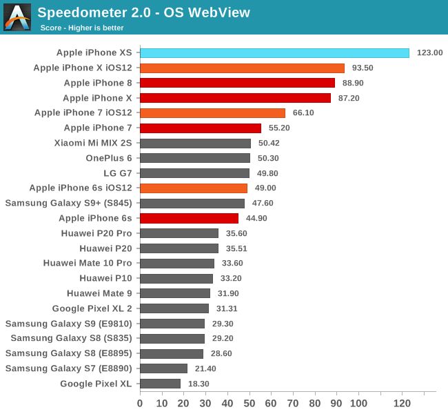
Speedometer 2.0 is the latest industry standard JavaScript benchmark, which can test the performance of the most common and modern JS frameworks.
Compared with the A11, the performance of the A12 has jumped by 31%, pointing out that the performance data in Apple's advertisement is far lower than the new chip.
We also see a slight improvement in iOS 12 on the previous generation of devices. This is not only due to changes in the way the iOS scheduler handles load, but also due to further improvements in every evolving JS engine used by Apple.

WebXPRT 3 is also a browser test, but its workload is more extensive and diversified, including a large number of processing tests. Here, the iPhone XS shows an 11% advantage over the iPhone X, which is slightly less advantageous than the Speedometer 2.0 test.
Previous devices have also seen steady performance improvements, with iPhone X’s score rising from 134 points to 147 points, or 10%. Compared with the A10 of the iPhone 7, there is a significant increase of 33%, which we will introduce in detail later.
IOS12 scheduler loading ramp analysis
Apple promises that the iOS12 system will have a significant performance improvement, thanks to the way their new scheduler calculates the load of a single task. The kernel scheduler of the operating system tracks the execution time of threads and aggregates it into a utilization indicator, which is then used by the DVFS mechanism and so on. The algorithm that determines how this load changes over time is usually a simple software decision-it can be adjusted and designed in a way that the supplier sees fit.
Because the core of iOS is closed source, we can't really see what the changes are, but we can measure their effects. A relatively simple method is to track the frequency of the workload from idle to highest performance. Before and after the iOS12 system upgrade, I conducted this test on iPhone 6 to X (and XS).

We started with the iPhone 6 with the A8 chipset, and I got some weird results on iOS11, because the rise characteristics from idle to maximum performance are very unusual. I repeated it several times, but the result is still the same. The CPU of A8 is 400MHz when idle, and stays here for 110ms until it jumps to 600MHz, and then stays for 10ms, entering the highest performance 1400MHz.
The iOS12 system showed a more stepped feature, which started to rise earlier and reached the highest performance after 90ms.

iPhone 6S has significantly different rise characteristics on iOS11, while the DVFS of the A9 chip is very slow. Here, the CPU needs a total of 435ms to reach its maximum frequency. With the update of iOS12, this time has been significantly reduced to 80ms, greatly improving the performance under a shorter interactive workload.
I was surprised to see how slow the scheduler used to be. This is the problem with the current Samsung Exynos chipset and other Android SoCs that do not optimize the scheduler. Although hardware performance may exist, it does not show up in short-term interactive workloads because the scheduler load tracking algorithm is too slow.

A10 and A9 have similar shortcomings, and the time to reach the highest performance exceeds 400ms. In the iOS12 system, iPhone 7 halved this speed, which is about 210ms. Compared with A9, A10 is more conservative in this respect, which is strange, but this may be related to the small core.
In this picture, we can also see the frequency of the small core Zephyr. They start at 400MHz and reach a peak at 1100MHz. The frequency in the figure drops back to 758MHz, because at this time one core switches to the large core, and then their frequencies continue to rise until they reach the highest performance.

On the Apple A11, I did not see any major changes. In fact, any difference may be the measurement of random noise between different firmwares. In iOS11 and iOS12, A11 rises to full frequency in about 105ms. Please note that the x-axis in this graph is much shorter than the previous graph.
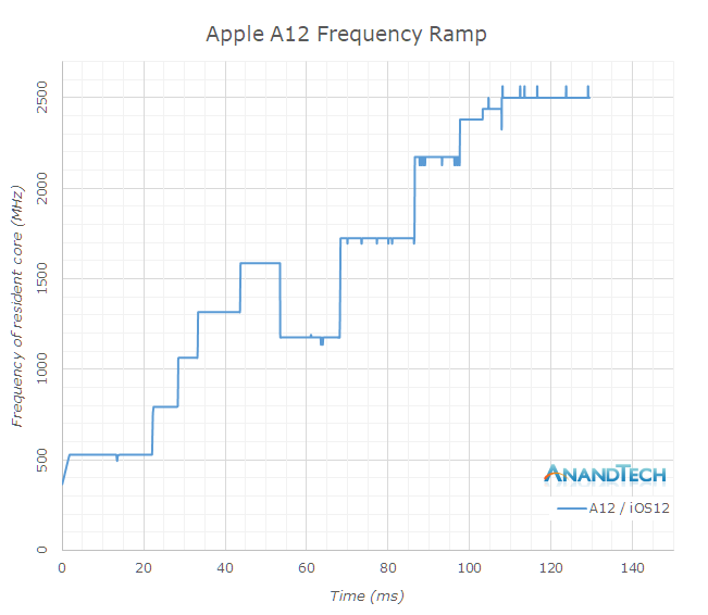
Finally, on the A12 chipset of the iPhone XS, we cannot measure any pre-update and post-update features, because the iPhone XS comes with iOS12. At this point, we once again saw that it reached the highest performance after 108ms, and we saw a trend from the Tempest core to the Vortex core.
In short, I hope this is the best and clear display of the performance difference iOS12 brings to old devices.
As far as the iPhone XS is concerned, I have no doubts about its performance, it is very fast. I have to admit that I am still an Android user, and my phone has completely turned off animations because I found that this would hinder the speed of the device. iOS cannot completely turn off animations. Although this is just my subjective personal opinion, I found that they seriously hinder the real performance of the phone. In non-interactive workloads, the iPhone XS just completed the test without any problems or exceptions.
GPU performance
The performance improvement of the A12 GPU is one of the biggest highlights of the speech. Compared with the A11 GPU, the performance has increased by 50%. Apple achieved this goal by "simply" adding a fourth GPU core to the A11's three GPUs and introducing memory compression on the GPU. I think that memory compression is the most helpful factor in improving the performance of the GPU's micro-architecture, because it is actually a huge one-time change. It is undeniable that Apple took a long time to complete.
Before entering the benchmark test, I would like to mention that the peak performance and peak power consumption of the latest Apple GPUs are a problem. We have seen that Apple has changed from a period of continuous performance improvement to one of the worst "criminals" from the decline in SoC peak performance to actual performance degradation. There are reasons for this, but I will talk about it soon.

The 3DMark physical test is mainly a CPU limit test, it also emphasizes the overall platform power limit, and the GPU is also working. We see that iPhone XS and A12 have made great progress compared to last year's iPhone. This is a test that was particularly problematic for Apple CPUs in the past, but this small micro-architecture problem seems to be solved in the A11 and Monsoon cores. The Vortex core and the always-increasing SoC power efficiency further improved performance, and finally matched the ARM core in this particular test.
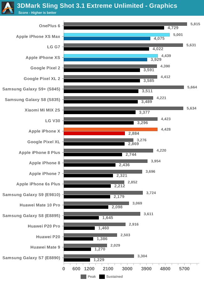
In the graphics part of the 3DMark test, the sustained performance of the iPhone XS was 41% higher than last year's iPhone X. In this particular test, OnePlus 6's more generous thermal element still allowed the Snapdragon 845 to perform better than the new chip.
In terms of peak performance, I ran into some big problems in 3DMark: I couldn't complete a run while keeping the iPhone XS or XS Max cool. If the device is cool enough, the GPU will increase to very high performance or even crash. I can always reproduce this phenomenon over and over again. I tried to measure the power in the test, and the instantaneous average power of the platform was 7-8 watts. For values ​​higher than 8, I suspect that this measurement method could not be recorded. GPU crash means that during operation, the power output cannot provide the necessary transient current, and we will see a voltage drop, causing the GPU to crash.
After repeating the test many times in several attempts, I heated the SoC until it decided to start at a lower GPU frequency, which allowed the test to be successfully completed.
GFXBench test
Kishonti recently released the new GFXBench 5 Aztec Ruins test, which brings newer, more modern, and more complex workloads to our test suite. In an ideal situation, we would test real games, but this is incredible on mobile devices, because basically no game has a built-in benchmarking mode. There are some tools that can collect fps values, but the biggest problem here is the repeatability of the workload when playing games manually, which is also a big problem in many online games today.

I still think that man-made benchmarks have a very solid position here, as long as you understand the characteristics of benchmarks. Kishonti's GFXBench has been the industry standard for many years, and the new Aztec test gave us a different workload. The new test coloring is thicker, using more complex effects to emphasize the computing power of the GPU. Although the data in the above table was collected on the Mali G72 GPU, it can still provide overall expectations for other architectures. The new test also requires bandwidth due to its larger texture.
Generally speaking, the correlation between the game and the benchmark depends on the percentage of various graphics workloads, whether there are large fills or coarse textures, whether they have complex geometric shapes, or just the coloring effects are becoming more and more complex. It needs GPU computing power.
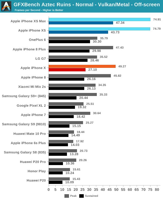
The Aztec Ruins in normal mode is a new and undemanding test. The new Apple A12 mobile phone exhibits extremely high peak performance, which is 51% higher than last year's iPhone.
In terms of sustained performance, the numbers dropped rapidly after a few minutes and then stabilized further. At this time, the performance of the iPhone XS is 61% higher than that of the iPhone X. Apple A12 can also beat the current leader OnePlus 6 Snapdragon 845 with a 45% advantage in sustained performance.
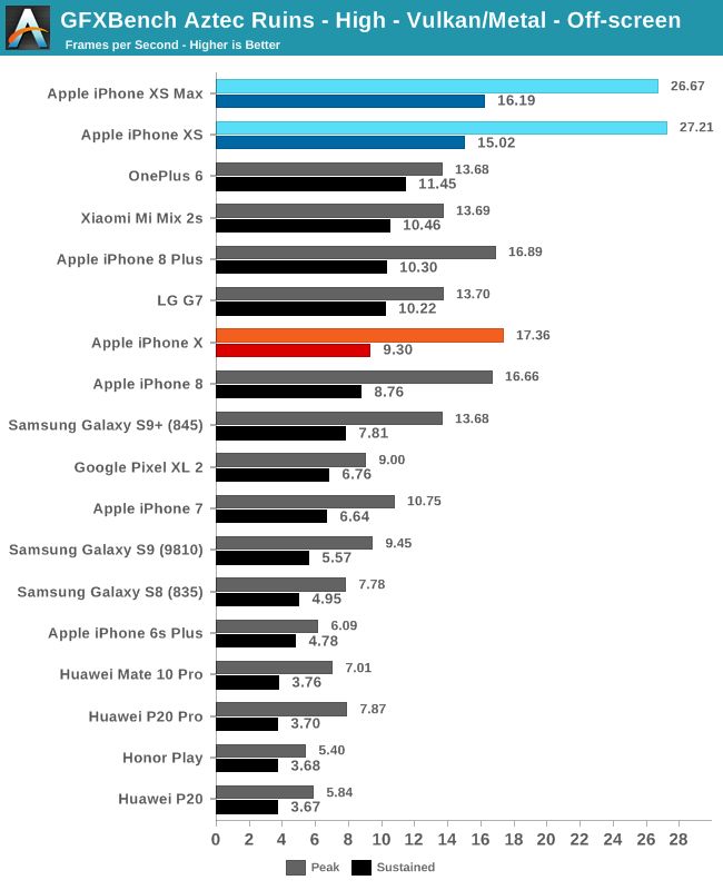
In the advanced mode of Aztec Ruins, we saw a surprisingly similar performance ranking. The peak performance of the iPhone XS is once again excellent, but the important thing is the continuous score. At this time, iPhone XS performance is 61% higher than iPhone X. The performance difference of OnePlus 6's Snapdragon 845 is reduced to 31% here, which is slightly lower than the normal mode. We may encounter some bottlenecks in some aspects of the micro-architecture.
GPU power
The platform and GPU features of Apple devices have always been things I want to publish, but they are very complicated to implement. I got reasonable data for the new iPhone XS, but the old SoC data still need to wait for the opportunity.
I don't have time to test Aztec Ruins on various devices, so we still rely on the standard Manhattan 3.1 and T-Rex. First, we first list the test results:

Similarly, in Manhattan 3.1, the performance of the new iPhone XS is 75% higher than that of the iPhone X. The improvement here is not only because of the improvement of the GPU micro-architecture, having an additional core, and the new SoC process node, but also because the new memory compression reduces the energy consumption of external DRAM, which can be used in heavy bandwidth 3D workloads. It accounts for 20-30% of system power consumption. The power savings on DRAM means that GPUs and SoCs can use more energy, thereby improving performance.

这里的功率数å—是系统的有效功率,表示总设备功率å‡åŽ»ç»™å®šå·¥ä½œè´Ÿè½½æƒ…况下的空闲功率(其ä¸åŒ…括å±å¹•åŠŸçŽ‡ï¼‰ã€‚
在峰值性能下,当设备在22°C环境温度下冷å´æ—¶ï¼Œè‹¹æžœA12çš„GPU会éžå¸¸è€—电,功率达到6W。这并ä¸æ˜¯GPUçš„å¹³å‡å³°å€¼ï¼Œå› 为我先å‰æ到过3DMark达到7.5Wå·¦å³ï¼ˆåœ¨å´©æºƒä¹‹å‰ï¼‰ã€‚
å³ä½¿åœ¨è¿™ä¸ªé«˜åŠŸçŽ‡æ•°å—下,A12的效率也超过了其他所有SoC。虽然这颇为有趣,但强调苹果的节æµç‰¹æ€§æ˜¯éžå¸¸é‡è¦çš„。在仅仅3分钟或3个基准测试è¿è¡ŒåŽï¼Œæ‰‹æœºå°†èŠ‚æµçº¦25%,达到我在效率表ä¸æ‰€è¯´çš„“温暖â€çŠ¶æ€ã€‚功率达到åˆç†çš„3.79W。值得注æ„的是,电æºæ•ˆçŽ‡å¹¶æ²¡æœ‰å¤§å¹…æ高,åªæ˜¯æ¯”峰值æ高了16%。这æ„味ç€è¯¥å¹³å°çš„功率曲线相对较低,并且性能å—到çƒé‡çš„é™åˆ¶ã€‚

接下æ¥çœ‹T-Rex,iPhone XSå†æ¬¡å±•ç¤ºäº†61ï¼…çš„æŒç»æ€§èƒ½æå‡ã€‚

我们看到,T-Rex的功耗与Manhattan的功耗一致,低温设备的峰值功率达到6W多一点。在è¿è¡Œ3次之åŽï¼Œå³°å€¼åŠŸçŽ‡å†æ¬¡é™ä½Žåˆ°4W以下,性能下é™äº†28%。这里的效率并没有太大的æ高,å†æ¬¡è¡¨æ˜ŽåŠŸçŽ‡æ›²çº¿ç›¸å¯¹è¾ƒä½Žã€‚
需è¦æ³¨æ„的是,“温暖â€è¿è¡Œçš„功率度é‡å¹¶ä¸ä»£è¡¨æŒç»çš„性能,我åªæ˜¯æƒ³åœ¨å³°å€¼æ•°æ®æ—è¾¹æ·»åŠ ä¸€ä¸ªé¢å¤–çš„æ•°æ®ç‚¹ã€‚大多数设备的æŒç»åŠŸçŽ‡åœ¨3-3.5W范围内。
为什么苹果公å¸åœ¨å³°å€¼æ€§èƒ½å’ŒæŒç»æ€§èƒ½ä¹‹é—´å˜åœ¨å¦‚æ¤å·¨å¤§çš„差异?先å‰ï¼ŒiPhone 6å’ŒA8å‘布的时候,æŒç»æ€§èƒ½ä¾¿æ˜¯è‹¹æžœçš„主è¦å…³æ³¨ç‚¹ä¹‹ä¸€ã€‚è¿™ç§å˜åŒ–是由于日常GPU用例å‘生了å˜åŒ–,以åŠè‹¹æžœå¦‚何将GPU用于与3Dæ— å…³çš„å·¥ä½œè´Ÿè½½ã€‚
Apple大é‡ä½¿ç”¨GPU计算,用于å„ç§ç”¨é€”,例如appä¸çš„ä¸€èˆ¬ç¡¬ä»¶åŠ é€Ÿã€ä½¿ç”¨GPU计算进行相机图åƒå¤„ç†ã€‚在这些用例ä¸ï¼ŒæŒç»çš„性能并ä¸é‡è¦ï¼Œå› 为它们是事务性工作负载,这æ„味ç€éœ€è¦å°½å¿«å¤„ç†çš„固定工作负载。
åœ¨è¿‡åŽ»çš„å‡ å¹´é‡Œï¼ŒAndroid GPU计算一直是一场彻头彻尾的ç¾éš¾ï¼Œæˆ‘主è¦æ˜¯å£°è®¨è°·æŒæ²¡æœ‰åœ¨AOSPä¸æ”¯æŒOpenCL,这使得供应商对OpenCL的支æŒéžå¸¸é›¶æ•£ã€‚RenderScriptä»ŽæœªèŽ·å¾—å¤ªå¤šçš„å…³æ³¨ï¼Œå› ä¸ºå®ƒä¸èƒ½ä¿è¯æ€§èƒ½ã€‚Android设备和SoC的碎片化æ„味ç€åœ¨ç¬¬ä¸‰æ–¹appä¸åŸºæœ¬ä¸å˜åœ¨GPU计算(如有错误,敬请指æ£ï¼ï¼‰
苹果对APIæ ˆçš„åž‚ç›´é›†æˆå’Œä¸¥æ ¼æŽ§åˆ¶æ„味ç€GPU计算æˆä¸ºäº†çŽ°å®žï¼Œè€Œäº‹åŠ¡æ€§GPUå³°å€¼æ€§èƒ½æ˜¯å€¼å¾—è€ƒè™‘çš„æŒ‡æ ‡ã€‚
现在,虽然这确实解释了节æµçš„åŽŸå› ï¼Œä½†æˆ‘ä»ç„¶è®¤ä¸ºè‹¹æžœå¯ä»¥åšä¸€äº›çƒä¼˜åŒ–。我在iPhone XS上玩了Fortnite游æˆï¼Œæ‰‹æœºçš„å‘çƒè®©æˆ‘ä¸æ˜¯å¾ˆå–œæ¬¢ã€‚æ¤æ—¶ï¼Œå¿…须有æŸç§æ–¹å¼æ¥è®©å…·æœ‰æŒç»æ€§èƒ½ç‰¹å¾çš„游æˆå’Œapp切实从GPU开始é™åˆ¶è¿™ç§æŒç»çš„性能状æ€ã€‚
除了çƒæ€§èƒ½å’Œå³°å€¼æ€§èƒ½çš„è€ƒè™‘å› ç´ ä»¥å¤–ï¼ŒiPhone XSå’ŒXS Max由于新的A12 SoC,展示出业界领先的性能和效率,并且目å‰æ˜¯æœ€å¥½çš„手机游æˆå¹³å°ã€‚
Fiber Fast Connector,Fiber Quick Connector,Fast Connect Fiber Connectors,Fiber Optic Quick Connector
Ningbo Fengwei Communication Technology Co., Ltd , https://www.fengweicommunication.com
